
User Manual

RF12B
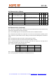
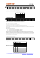
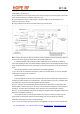
Control Commands
Control Command Related Parameters/Functions Related control bits
1 Configuration Setting Command
Frequency band, crystal oscillator load capacitance,
baseband filter bandwidth, etc.
el, ef, b1 to b0, x3 to x0
2 Power Management Command
Receiver/Transmitter mode change, synthesizer, xtal osc,
PA, wake-up timer, clock output can be enabled here
er, ebb, et, es, ex, eb,
ew, dc
3 Frequency Setting Command Data frequency of the local oscillator/carrier signal f11 to f0
4 Data Rate Command Bit rate cs, r6 to r0
5 Receiver Control Command
Function of pin 16, Valid Data Indicator, baseband bw, LNA
gain, digital RSSI threshold
p16, d1 to d0, i2 to i0,
g1 to g0, r2 to r0
6 Data Filter Command Data filter type, clock recovery parameters al, ml, s1 to s0, f2 to f0
7 FIFO and Reset Mode Command
Data FIFO IT level, FIFO start control, FIFO enable and
FIFO fill enable
f3 to f0, s1 to s0, ff, fe
8 Receiver FIFO Read Command RX FIFO can be read with this command
9 Synchron Pattern Command Synchron pattern b7 to b0
10 AFC Command A F C p a r a m e t e r s
a1 to a0, rl1 to rl0, st, fi,
oe, en
11 TX Configuration Control Command Modulation parameters, output power, ea mp, m3 to m0, p2 to p0
12 PLL Setting Command
CLK out buffer speed, low power mode of the crystal
oscillator, dithering, PLL loop delay, bandwidth
ob1 to ob0, lpx, ddit,
ddy, bw1 to bw0
13
Transmitter Register Write
Command
TX data register can be written with this command t7 to t0
14 Wake-Up Timer Command Wake-up time period r4 to r0, m7 to m0
15 Low Duty-Cycle Command Enable low duty-cycle mode. Set duty-cycle. d6 to d0, en
16
Low Battery Detector and
Microcontroller Clock Divider
Command
LBD voltage and microcontroller clock division ratio d2 to d0, v4 to v0
17 Status Read Command Status bits can be read out
In general, setting the given bit to one will activate the related function. In the following tables, the
POR column shows the default values of the command registers after power-on.
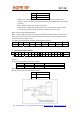
Description of the Control Commands
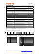
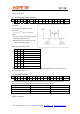
1. Configuration Setting Command
bit 15 14 13 12 11 10 9 8 7 6 5 4 3 2 1 0 POR
1 0 0 0 0 0 0 0 el ef b1 b0 x3 x2 x1 x0 8008h
Bit el enables the internal data register. If the data register is used the FSK pin must be connected to logic high level.
Bit ef enables the FIFO mode. If ef=0 then DATA (pin 6) and DCLK (pin 7) are used for data and data clock output.
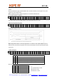
x3 x2 x1 x0 Crystal Load Capacitance [pF]
0 0 0 0 8.5
0 0 0 1 9.0
0 0 1 0 9.5
0 0 1 1 10.0
…
1 1 1 0 15.5
1 1 1 1 16.0
b1 b0 Frequency Band [MHz]
0 0 Reserved
0 1 433
1 0 868
1 1 915
Tel: +86-755-86096587 Fax: +86-755-86096602 E-mail: sales@hoperf.com http://www.hoperf.com