
User Manual

RF12B
Tel: +86-755-86096587 Fax: +86-755-86096602 E-mail: sales@hoperf.com http://www.hoperf.com
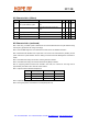
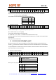
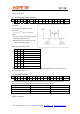
AC Characteristics (Others)
Symbol Parameter Conditions/Notes Min Typ Max Units
C
xl
Crystal load capacitance,
see crystal selection guide
Programmable in 0.5 pF steps, tolerance
+/- 10%
8.5 16 pF
t
POR
Internal POR timeout
A
fter Vdd has reached 90% of final value
(Note 9)
100 ms
t
PBt
Wake-up timer clock period
Calibrated every 30 seconds
0.95 1.05 ms
C
in, D
Digital input capacitance
2 pF
t
r, f
Digital output rise/fall time
15 pF pure capacitive load
10 ns
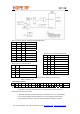
AC Characteristics (continued)
Note 1: Not using a 10 MHz crystal is allowed but not recommended because all crystal referred timing
and frequency parameters will change accordingly.
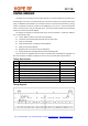
Note 2: See the BER diagrams in the measurement results section for detailed information.
Note 3: Measured with disabled clock output buffer. This current can be decreased by enabling the low
power mode of the crystal oscillator. See PLL Setting Command and Power Management Command for
details.
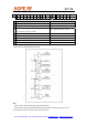
Note 4: See Reference design with 50 Ohm matching network for details.
Note 5: See Reference design with resonant PCB antenna (BIFA) for details.
Note 6: Supposing identical antenna with RF12B in RX mode, the outdoor RF link range will be
approximately 120 meters indoor and 450 meters outdoor.
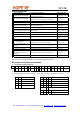
Note 7: Optimal antenna admittance/impedance:
RF12B Yantenna [S] Zantenna [Ohm] Lantenna [nH]
433 MHz 1.4E-3 - j7.1E-3 27 + j136 52.00
868 MHz 2E-3 - j1.5E-2 8.7 + j66 12.50
915 MHz 2.2E-3 - j1.55E-2 9 + j63 11.20
Note 8: Adjustable in 8 steps.
Note 9: During this period, commands are not accepted by the chip.