
User Manual

RF01
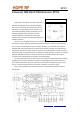
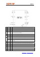
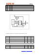
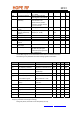
PACKAGE PIN DEFINITIONS
Pin type key: D=digital, A=analog, S=supply, I=input, O=output, IO=input/output
Pin Name Type Function
1 SDI DI Data input of serial control interface
2 SCK DI Clock input of serial control interface
3 nSEL DI Chip select input of three-wire control interface (active low)
4 FFIT/SD
O
DO
FIFO IT (active low) or serial data out for Status Read Command.
Tristate with bushold cell if nSEL=H
5 nIRQ DO Interrupt request output, (active low)
DATA DO Received data output (FIFO not used)
6
nFFS DI FIFO select input
DCLK DO Received data clock output (Digital filter used, FIFO not used)
CFIL AIO External data filter capacitor connection (Analog filter used)
7
FFIT DO
FIFO IT (active high) FIFO empty function can be achieved when FIFO IT level is
set to one
8 CLK DO Clock output for the microcontroller
9 XTL/RE
F
AIO Crystal connection (other terminal of crystal to VSS) / External reference input
10 nRES DO Reset output (active low)
11 VSS_D S Digital VSS(connect to VSS)
12 VSS_A S Analog VSS(connect to VSS)
13 VSS_LN
A
S LNA VSS(connect to VSS)
14 IN2 AI RF differential signal input
15 IN1 AI RF differential signal input
Tel: +86-755-86096587 Fax: +86-755-86096602 E-mail: sales@hoperf.com http://www.hoperf.com