
User Manual

RF01
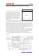
CONTROL INTERFACE
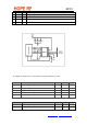
Commands to the receiver are sent serially. Data bits on pin SDI are shifted into the device upon the
rising edge of the clock on pin SCK whenever the chip select pin nSEL is low. When the nSEL signal is
high, it initializes the serial interface. The number of bits sent is an integer multiple of 8. All commands
consist of a command code, followed by a varying number of parameter or data bits. All data are sent
MSB first (e.g. bit 15 for a 16-bit command). Bits having no influence (don’t care) are indicated with X.
The Power On Reset (POR) circuit sets default values in all control registers.
The receiver will generate an interrupt request (IRQ) for the microcontroller on the following events:
z Supply voltage below the preprogrammed value is detected (LBD)
z Wake-up timer timeout (WK-UP)
z FIFO received the preprogrammed amount of bits (FFIT)
z FIFO overflow (FFOV)
FFIT and FFOV are applicable only when the FIFO is enabled. To find out why the nIRQ was issued, the
status bits should be read out.
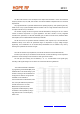
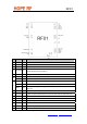
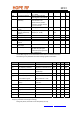
Timing Specification
Symbol Parameter Minimum Value [ns]
t
CH
Clock high time 25
t
CL
Clock low time 25
t
SS
Select setup time (nSEL falling edge to SCK rising edge) 10
t
SH
Select hold time (SCK falling edge to nSEL rising edge) 10
t
SHI
Select high time 25
t
DS
Data setup time (SDI transition to SCK rising edge) 5
t
DH
Data hold time (SCK rising edge to SDI transition) 5
t
OD
Data delay time 10
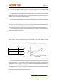
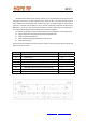
Timing Diagram
Tel: +86-755-86096587 Fax: +86-755-86096602 E-mail: sales@hoperf.com http://www.hoperf.com