
Owner manual


RC2100
2005 Radiocrafts AS RC2100 Data Sheet (rev. 1.0) Page 21 of 22
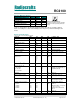
30 – 1000 MHz
1 – 12.75 GHz
-57
-47
dBm 300 440, FCC CFR47 Part 15
and ARIB STD-T66
Supply voltage
2.8 5.5 V
Supply voltage rise time 150 us If appropriate rise time can not
be guaranteed, the RESET pin
should be activated after
supply voltage is stable.
Current consumption, RX/IDLE
21.4
mA
Apply over entire supply
voltage range
Current consumption, TX
Power level 1: -27 dBm
2: -17 dBm
3: -12 dBm
4: -7 dBm
5: -2 dBm
9.7
10.9
12.1
14.5
18.0
mA
Apply over entire supply
voltage range
Current consumption, SLEEP 85
150
µA Max value in bold apply over
the entire temperature and
supply voltage range
Current consumption, OFF
0.003
1.5
µA Max value in bold apply over
the entire temperature and
supply voltage range
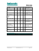
Digital I/O
Input logic level, low
Input logic level, high
Output logic level, low (1µA)
Output logic level, high(-1µA)
1.7
0
2.6
0.7
5.5
0.1
2.7
V
RXEN, TXEN, CONFIG, TXD
and RXD have internal 100 k
series resistors. No internal
pull-ups. Outputs should not be
loaded resistively.
RESET pin
Input logic level, low
Input logic level, high
1.7
0.7
2.7
V
Internal 100 k
pull-up resistor
to VDD
ON/OFF pin
Input logic level, low
Input logic level, high
1.4
0.4
VCC
V
No internal pull-up resistor
Document Revision History
Document Revision Changes
1.0 First release