
User guide
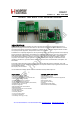

RAM01
Version: 1.0 Date: 10/11/2008
Tel: +86-755-82973805 Fax: +86-755-82973550 E-mail: sales@hoperf.com http://www.hoperf.com
4
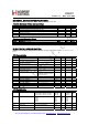
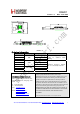
BR = 9.6 kbps, Average signal
power
IIP3outh Input IP3 out of band interferers
f-f
LO > 5MHz
-18 dBm
CCR Co-channel rejection BER = 10-2 with continuous wave
interferer in the channel
-4 dB
BR100kHz Blocking ratio BER = 10-2 with continuous wave
interferer, BW = 85 kHz,
interferer offset 100 kHz
45 dB
BR1MHz Blocking ratio same as above,
interferer offset 1 MHz
50 dB
BR10MHz Blocking ratio same as above,
interferer offset 10 MHz
67 dB
Pmaxh Maximum input power LNA: high setting
min 99.99% OOK modulation
-15 dBm
Pmaxa Maximum input power LNA: automatic or low gain setting
min 99.9% OOK modulation
0 dBm
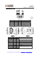
Rin RF input impedance real
part (differential) (Note 1)
250 Ohm
Cin RF input capacitance 460 fF
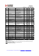
RSa RSSI accuracy +/-7 dB
RSr RSSI range With automatic 32 dB LNA gain
switch
90 dB
RSresp DRSSI response time Until the RSSI output goes high
after the input signal exceeds the
preprogrammed
limit, C
ARRSI = 5nF
500 μs
fref PLL reference frequency (Note 2)
10
MHz
fresLB PLL frequency resolution 434 MHz Band 10 kHz
fresHB PLL frequency resolution 868 MHz or 915 MHz Band 20 kHz
Tsettl PLL settling time Frequency error < 1 kHz
after 1 MHz step
30 μs
tst1, P PLL startup time Initial calibration after power-up with
running crystal oscillator
500 μs
Pspur Spurious emission -60 dBm
Cxl Crystal load capacitance,
see crystal selection guide
Programmable in 0.5 pF steps,
tolerance +/- 10%
8.5
16 pF
tPOR Internal POR pulse width
(Note 3)
After Vdd has reached 90% of final
value
50 100 ms
tsx Crystal oscillator startup
time
Crystal ESR < 30 Ω 5 ms
tPBt Wake-up timer clock period Calibrated every 30 seconds (Note
4)
0.995 1 1.005 ms
twake-up Programmable wake-up
time
1
8.4*10
6
ms
Cin, D Digital input capacitance 2 pF
tr, f Digital output rise/fall time 15 pF pure capacitive load 10 ns
tr, f ,ckout Clock output rise/fall time 10 pF pure capacitive load 15 ns
fckout, slow Slow clock frequency Tolerance +/- 1 kHz 32 kHz
Note 1: See matching circuit parameters and antenna design guide for information, and Application Notes available
from http://www.hoperf.com.
Note 2: Using other than a 10 MHz crystal is not recommended because the crystal referred timing and frequency
parameters will change accordingly.
Note 3: During this period, commands are not accepted by the chip.
Note 4: Autocalibration can be turned off.