
User Manual


SECTION 4
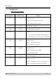
1. Configuration
1.1. Solder pads configuration
Designation Default setting Feature
JP2 closed NAND chip select
opened: Nand chip select not wired
closed: Nand chip select wired
JP3 closed Phy IRQ line connection
JP4 closed User Push-button connection
JP5 1-2 VDDBU
1-2: 1.8V from the low dropout voltage regulator
2-3: VBAT signal on J1.3 (through the LP3990MF)
JP6 opened JTAG selection
opened: Embedded ICE mode
closed: Boundary scan mode
JP7 opened Boot Mode select
opened: boot from internal ROM
closed: boot from NCS0
JP8 closed User Led connection
JP9 opened Nand write protect
opened: nand flash write protection disabled
closed: nand flash write protection enabled
Datasheet USG-00006-A01 12/20