
Owner's manual
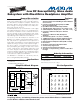


MAX9877
Low RF Susceptibility, Mono Audio
Subsystem with DirectDrive Headphone Amplifier
6 _______________________________________________________________________________________
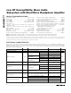
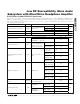
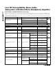
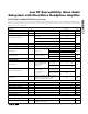
ELECTRICAL CHARACTERISTICS (continued)
(V
DD
= PV
DD
= 3.7V, V
GND
= V
PGND
= 0V. Single-ended inputs, preamp gain = 0dB, volume controls = 0dB, OSC = 00, BYPASS = 0,
SHDN = 1. Speaker loads (Z
SPK
) connected between OUT+ and OUT-. Headphone loads (R
HP
) connected from HPL or HPR to GND.
SDA and SCL pullup voltage = 3.3V. Z
SPK
= ∞, R
HP
= ∞. C1 = C2 = C
BIAS
= 1µF. T
A
= T
MIN
to T
MAX
, unless otherwise noted. Typical
values are at T
A
= +25°C.) (Note 3)
PARAMETER SYMBOL CONDITIONS MIN TYP MAX UNITS
2-WIRE INTERFACE TIMING
External Pullup Voltage Range:
SDA and SCL
1.7 3.6 V
Serial Clock Frequency f
SCL
DC 400 kHz
Bus Free Time Between STOP
and START Conditions
t
BUF
1.3 µs
START Condition Hold t
HD:STA
0.6 µs
START Condition Setup Time t
SU:STA
0.6 µs
Clock Low Period t
LOW
1.3 µs
Clock High Period t
HIGH
0.6 µs
Data Setup Time t
SU:DAT
100 ns
Data Hold Time t
HD:DAT
0 900 ns
Maximum Receive SCL/SDA Rise
Time
t
R
300 ns
Maximum Receive SCL/SDA Fall
Time
t
F
300 ns
Setup Time for STOP Condition t
SU:STO
0.6 µs
Capacitive Load for Each Bus
Line
C
b
400 pF
Note 3: All devices are 100% production tested at room temperature. All temperature limits are guaranteed by design.
Note 4: Amplifier inputs are AC-coupled to GND.
Note 5: Output levels higher than 825mW are not recommended for extended durations. Production tested with Z
SPK
= 8Ω + 68µH only.