
Manual

Stereo Audio Codec
with FLEXSOUND Technology
MAX98088
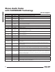
57
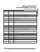
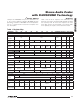
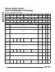
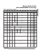
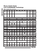
Table 1. Register Map
I
2
C Slave Address
Configure the MAX98088 using the I
2
C control bus. The
IC uses a slave address of 0x20 or 00100000 for write
operations and 0x21 or 00100001 for read operations.
See the I
2
C Serial Interface section for a complete inter-
face description.
Registers
Table 1 lists all of the registers, their addresses, and
power-on-reset states. Registers 0x00 to 0x03 and 0xFF
are read-only while all of the other registers are read/
write. Write zeros to all unused bits in the register table
when updating the register, unless otherwise noted.
REGISTER B7 B6 B5 B4 B3 B2 B1 B0 ADDRESS DEFAULT R/W PAGE
STATUS
Status CLD SLD ULK — — — JDET — 0x00 — R 111
Microphone
AGC/NG
NG AGC 0x01 — R 70
Jack Status — JKSNS — — — — — — 0x02 — R 110
Battery
Voltage
— — — VBAT 0x03 — R/W 110
Interrupt
Enable
ICLD ISLD IULK 0 0 0 IJDET 0 0x0F 0x00 R/W 111
MASTER CLOCK CONTROL
Master Clock 0 0 PSCLK 0 0 0 0 0x10 0x00 R/W 81
DAI1 CLOCK CONTROL
Clock Mode SR1 FREQ1 0x11 0x00 R/W 81, 82
Any Clock
Control
PLL1 NI1[14:8] 0x12 0x00 R/W 82
NI1[7:1] NI1[0] 0x13 0x00 R/W 82
DAI1 CONFIGURATION
Format MAS1 WCI1 BCI1 DLY1 0 TDM1 FSW1 WS1 0x14 0x00 R/W 76
Clock ADC_OSR1
DAC_ORS1
0 0 BSEL1 0x15 0x00 R/W 77
I/O
Configuration
SEL1 LTEN1 LBEN1 DMONO1 HIZOFF1 SDOEN1 SDIEN1 0x16 0x00 R/W 77, 78
Time-Division
Multiplex
SLOTL1 SLOTR1 SLOTDLY1 0x17 0x00 R/W 78
Filters MODE1 AVFLT1 DHF1 DVFLT1 0x18 0x00 R/W 86
DAI2 CLOCK CONTROL
Clock Mode SR2 0 0 0 0 0x19 0x00 R/W 81
Any Clock
Control
PLL2 NI2[14:8] 0x1A 0x00 R/W 82
NI2[7:1] NI2[0] 0x1B 0x00 R/W 82
DAI2 CONFIGURATION
Format MAS2 WCI2 BCI2 DLY2 0 TDM2 FSW2 WS2 0x1C 0x00 R/W 76
Clock 0 0
DAC_
ORS2
0 0 BSEL2 0x1D 0x00 R/W 77
I/O
Configuration
SEL2 0 LBEN2 DMONO2 HIZOFF2 SDOEN2 SDIEN2 0x1E 0x00 R/W 77, 78