
Manual
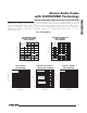

Stereo Audio Codec
with FLEXSOUND Technology
MAX98088
54
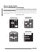
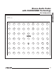
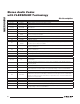
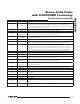
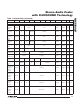
Pin Description
PIN NAME FUNCTION
A1, B1 SPKRN Negative Right-Channel Class D Speaker Output
A2, B2 SPKRGND Right-Speaker Ground
A3, B3 SPKLVDD
Left-Speaker, REF, Receiver Amp Power Supply. Bypass to SPKLGND with a 1FF and a
10FF capacitor.
A4, B4 SPKLP Positive Left-Channel Class D Speaker Output
A5, B5 SPKLN Negative Left-Channel Class D Speaker Output
A6
RECP/LOUTL/
RXINP
Positive Receiver Amplifier Output or Left Line Output. Can be positive bypass switch input
when receiver amp is shut down.
A7 PVDD
Headphone Power Supply. Bypass to HPGND with a 1FF capacitor.
A8 HPVSS
Inverting Charge-Pump Output. Bypass to HPGND with a 1FF ceramic capacitor.
A9 HPGND Headphone Ground
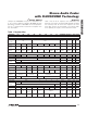
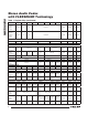
B6
RECN/LOUTR/
RXINN
Negative Receiver Amplifier Output or Right Line Output. Can be negative bypass switch
input when receiver amp is shut down.
B7 C1P
Charge-Pump Flying Capacitor Positive Terminal. Connect a 1FF ceramic capacitor
between C1N and C1P.
B8 C1N
Charge-Pump Flying Capacitor Negative Terminal. Connect a 1FF ceramic capacitor
between C1N and C1P.
B9 HPVDD
Noninverting Charge-Pump Output. Bypass to HPGND with a 1FF ceramic capacitor.
C1, C2 SPKRP Positive Right-Channel Class D Speaker Output
C3, D3 SPKRVDD
Right-Speaker Power Supply. Bypass to SPKRGND with a 1FF capacitor.
C4, C5 SPKLGND Left-Speaker Ground
C6, C7, D5, D6,
D7, E3
N.C. No Connection
C8 HPSNS
Headphone Amplifier Ground Sense. Connect to the headphone jack ground terminal or
connect to ground.
C9 HPL Left-Channel Headphone Output
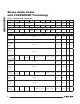
D1 BCLKS1
S1 Digital Audio Bit Clock Input/Output. BCLKS1 is an input when the ICs are in slave mode
and an output when in master mode. The input/output voltage is referenced to DVDDS1.
D2 SDOUTS1 S1 Digital Audio Serial-Data ADC Output. The output voltage is referenced to DVDDS1.
D4 LRCLKS1
S1 Digital Audio Left-Right Clock Input/Output. LRCLKS1 is the audio sample rate clock
and determines whether S1 audio data is routed to the left or right channel. In TDM mode,
LRCLKS1 is a frame sync pulse. LRCLKS1 is an input when the IC is in slave mode and an
output when in master mode.
D8 INB2 Single-Ended Line Input B2. Also positive differential line input B.
D9 HPR Right-Channel Headphone Output
E1 DVDDS1
S1 Digital Audio Interface Power-Supply Input. Bypass to DGND with a 1FF capacitor.
E2 MCLK Master Clock Input. Acceptable input frequency range is 10MHz to 60MHz.
E4 SDINS1
S1 Digital Audio Serial-Data DAC Input. The input/output voltage is referenced to DVDDS1.
The input voltage is referenced to DVDDS1.