
User guide


MAX9750/MAX9751/MAX9755
2.6W Stereo Audio Power Amplifiers and
DirectDrive Headphone Amplifiers
_______________________________________________________________________________________ 5
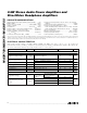
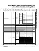
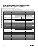
ELECTRICAL CHARACTERISTICS (continued)
(V
DD
= PV
DD
= CPV
DD
= HPV
DD
= 5V, GND = PGND = CPGND = 0V, SHDN = V
DD
, C
BIAS
= 1µF, C1 = C2 = 1µF, speaker load
terminated between OUT_+ and OUT_-, headphone load terminated between HPOUT_ and GND, GAIN1 = GAIN2 = VOL = GAIN = 0V,
T
A
= T
MIN
to T
MAX
, unless otherwise noted. Typical values are at T
A
= +25°C.) (Note 1)
PARAMETER
SYMBOL
CONDITIONS
MIN TYP MAX
UNITS
LOGIC INPUT (SHDN, GAIN1, GAIN2, GAIN, VOL, IN1/2)
Logic Input High Voltage V
IH
2V
Logic Input Low Voltage V
IL
0.8 V
Logic Input Current I
IN
±1µA
LOGIC INPUT HEADPHONE (HPS)
Logic Input High Voltage V
IH
2V
Logic Input Low Voltage V
IL
0.8 V
Logic Input Current I
IN
10 µA
Note 1: All devices are 100% production tested at room temperature. All temperature limits are guaranteed by design.
Note 2: Guaranteed by design. Not production tested.
Note 3: PSRR is specified with the amplifier input connected to GND through C
IN
.
Note 4: Output power levels are measured with the thin QFN’s exposed paddle soldered to the ground plane.
Note 5: See Table 3 for details of the mute levels.
Note 6: The value of R
B
dictates the minimum beep signal amplitude (see the Beep Input section).