
User guide


MAX9700
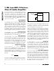
One solution is the configuration shown in Figure 10b.
The potentiometer is connected between the differential
inputs, and these “see” identical RC paths when the
device powers up. The variable resistive element
appears between the two inputs, meaning the setting
affects both inputs the same way. The potentiometer is
audio taper, as in Figure 10a. This significantly
improves transient performance on power-up or release
from SHDN. A similar approach can be applied when
the MAX9700 is driven differentially and a volume con-
trol is required.
UCSP Applications Information
For the latest application details on UCSP construction,
dimensions, tape carrier information, PC board tech-
niques, bump-pad layout, and recommended reflow tem-
perature profile, as well as the latest information on
reliability testing results, refer to the Application Note:
UCSP—A Wafer-Level Chip-Scale Package available on
Maxim’s website at www.maxim-ic.com/ucsp.
1.2W, Low-EMI, Filterless,
Class D Audio Amplifier
14 ______________________________________________________________________________________
Figure 10a. Single-Ended Drive of MAX9700 Plus Volume
IN+
1µF
1µF
MAX9700
IN-
CW
50kΩ
IN+
MAX9700
IN-
1µF
1µF
CW
22kΩ
50kΩ
22kΩ
Figure 10b. Improved Single-Ended Drive of MAX9700 Plus
Volume
Ordering Information (continued)
PART TEMP RANGE
PIN-
PACKAGE
TOP
MARK
MAX9700CETB* -40
o
C to +85
o
C 10 TDFN ACN
MAX9700CEUB* -40
o
C to +85
o
C 10 µMAX —
MAX9700CEBC-T* -40
o
C to +85
o
C 12 UCSP-12 —
MAX9700DETB* -40
o
C to +85
o
C 10 TDFN ACO
MAX9700DEUB* -40
o
C to +85
o
C 10 µMAX —
MAX9700DEBC-T* -40
o
C to +85
o
C 12 UCSP-12 —
Selector Guide
PART PIN-PACKAGE GAIN (dB)
MAX9700AETB 10 TDFN 6
MAX9700AEUB 10 µMAX 6
MAX9700AEBC-T 12 UCSP-12 6
MAX9700BETB 10 TDFN 12
MAX9700BEUB 10 µMAX 12
MAX9700BEBC-T 12 UCSP-12 12
MAX9700CETB 10 TDFN 15.6
MAX9700CEUB 10 µMAX 15.6
MAX9700CEBC-T 12 UCSP-12 15.6
MAX9700DETB 10 TDFN 20
MAX9700DEUB 10 µMAX 20
MAX9700DEBC-T 12 UCSP-12 20
*Future Product—contact factory for availability.