
Manual


MAX9670/MAX9671
Low-Power Audio/Video Switch with Audio
Volume Control for Dual SCART Connectors
6 _______________________________________________________________________________________
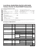
ELECTRICAL CHARACTERISTICS (continued)
(V
12
= 12V, V
VID
= V
AUD
= 3.3V, V
GNDVID
= V
EP
= 0V, no load, T
A
= 0°C to +70°C, unless otherwise noted. Typical values are at
T
A
= +25°C.) (Note 1)
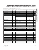
PARAMETER SYMBOL CONDITIONS MIN TYP MAX UNITS
Input Current 70 100 µA
Output Low Voltage 10kΩ to EP, 11.4V ≤ V
12
≤ 12.6V 1.5 V
Output Medium Voltage 10kΩ to EP, 11.4V ≤ V
12
≤ 12.6V 5 6.5 V
Output High Voltage 10kΩ to EP, 11.4V ≤ V
12
≤ 12.6V 10 V
DIGITAL INTERFACE
Input High Voltage V
IH
0.7 x
V
VID
V
Input Low Voltage V
IL
0.3 x
V
VID
V
Input Hysteresis V
HYS
0.06 x
V
VID
V
Input Leakage Current I
IH
, I
IL
T
A
= +25°C -1 +1 µA
Input Capacitance 6pF
Input Current
0.1V
VID
< SDA < 3.3V,
0.1V
VID
< SCL < 3.3V
I/O pins of fast-mode devices must not
obstruct the SDA and SCL lines if V+ is
switched off, T
A
= +25°C
-10 +10 µA
Output Low Voltage SDA V
OL
I
SINK
= 6mA 0.4 V
Serial-Clock Frequency f
SCL
0 400 kHz
Bus Free Time Between a STOP
and a START Condition
t
BUF
1.3 µs
Hold Time, (Repeated) START
Condition
t
HD
,
STA
0.6 µs
Low Period of the SCL Clock t
LOW
1.3 µs
High Period of the SCL Clock t
HIGH
0.6 µs
Setup Time for a Repeated
START Condition
t
SU
,
STA
0.6 µs
Data Hold Time t
HD
,
DAT
(Note 4) 0 0.9 µs
Data Setup Time t
HD
,
DAT
100 ns
Fall Time of SDA Transmitting t
F
I
SINK
≤ 6mA, C
B
= total capacitance of one
bus line in pF, t
R
and t
F
measured between
0.3V
VID
and 0.7V
VID
100 ns
Setup Time for STOP Condition t
SU
,
STO
0.6 µs
Pulse Width of Spike Suppressed t
SP
Input filters on the SDA and SCL inputs
suppress noise spikes less than 50ns
050ns