
Manual

MAX9655/MAX9656
Low-Power Video Switches
for Dual SCART Connectors
2 _______________________________________________________________________________________
ABSOLUTE MAXIMUM RATINGS
ELECTRICAL CHARACTERISTICS
(V
DD
= 3.3V, V
GND
= 0, V
SHDN
= V
DD
, VCR_SEL = V
DD
, TV_SEL = V
DD
, R
L
= 150Ω to GND, T
A
= T
MIN
to T
MAX
, unless otherwise
noted. Typical values are at T
A
= +25°C.) (Note 1)
Stresses beyond those listed under “Absolute Maximum Ratings” may cause permanent damage to the device. These are stress ratings only, and functional
operation of the device at these or any other conditions beyond those indicated in the operational sections of the specifications is not implied. Exposure to
absolute maximum rating conditions for extended periods may affect device reliability.
Supply Voltage
V
DD
to GND...........................................................-0.3V to +4V
All Video and Logic Input Pins..................(GND - 0.3V) to +4V
Duration of Output Short Circuit to V
DD
or GND ........Continuous
Continuous Input Current
All Video and Logic Input Pins .....................................±20mA
Continuous Power Dissipation (T
A
= +70°C)
16-Pin QSOP (derate 8.3mW/°C above +70°C)............667mW
20-Pin QSOP (derate 9.1mW/°C above +70°C)............727mW
Operating Temperature Range .........................-40°C to +125°C
Junction Temperature......................................................+150°C
Storage Temperature Range .............................-65°C to +150°C
Lead Temperature (soldering, 10s) .................................+300°C
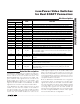
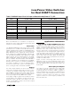
PARAMETER SYMBOL CONDITIONS MIN TYP MAX UNITS
Supply Voltage Range V
DD
Guaranteed by power-supply rejection test 2.7 3.3 3.6 V
Quiescent Supply Current I
DD
No load 21 45 mA
Shutdown Supply Current I
SHDN
V
SHDN
= 0 (MAX9656 only) 35 µA
Input Voltage Unselected input V
DD
/3 V
Input Resistance
Unselected input 222 kΩ
Sync-Tip Clamp Level V
CLP
0.23 0.3 0.39 V
2.7V ≤ V
DD
≤ 3.6V 1.05
Input Voltage Range
Guaranteed by output-
voltage swing
3.0V ≤ V
DD
≤ 3.6V 1.2
V
P-P
Sync Crush
Sync-tip clamp; percentage reduction in
sync pulse (0.3V
P-P
); guaranteed by input
clamping current measurement
2%
Input Clamping Current 12µA
Maximum Input Source
Resistance
300 Ω
V
DD
= 2.7V, 0V ≤ V
IN
≤ 1.05V
1.96 2 2.04
DC Voltage Gain A
V
R
L
= 150Ω to GND
(Note 2) V
DD
= 3.0V, 0V ≤ V
IN
≤ 1.2V
1.96 2 2.04
V/V
DC Gain Mismatch Guaranteed by output-voltage swing -2 +2 %
Output Level Measured at output, C
IN_
= 0.1µF to GND 0.218 0.3 0.39 V
Measured at output, V
DD
= 2.7V, V
IN
=
V
CLP
to (V
CLP
+1.05V), R
L
= 150Ω to -0.2V
2.1
Measured at output, V
DD
= 2.7V, V
IN
=
V
CLP
to (V
CLP
+1.05V), R
L
= 150Ω to V
DD
/2
2.1
Measured at output, V
DD
= 3.0V, V
IN
=
V
CLP
to (V
CLP
+1.2V), R
L
= 150Ω to -0.2V
2.4
Measured at output, V
DD
= 3.0V, V
IN
=
V
CLP
to (V
CLP
+1.2V), R
L
= 150Ω to V
DD
/2
2.4
Output-Voltage Swing
Measured at output, V
DD
= 3.135V, V
IN
=
V
CLP
to (V
CLP
+1.05V), R
L
= 75Ω to -0.2V
2.1
V
P-P