
User guide

MAX9532
DirectDrive Video Amplifier with
Short-to-Battery Protection
_______________________________________________________________________________________ 3
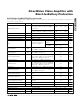
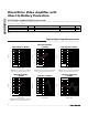
PARAMETER SYMBOL CONDITIONS MIN TYP MAX UNITS
Measured at output, V
DD
= 3.135V,
V
IN
= V
CLP
to (V
CLP
+ 0.7V), R
L
= 100Ω to
-2V and +2V
2.744 2.8 2.856
Output Voltage Swing
Measured at output, V
DD
= 3V, V
IN
= V
CLP
to (V
CLP
+ 0.5V), R
L
= 100Ω to -2V and +2V
1.96 2 2.04
V
P-P
Output Short-Circuit Current 90 mA
Output Resistance R
OUT
0.1 Ω
Short Circuit to Battery Current Short-to-battery, V
OUT
= 9V to 16V 3 mA
Power-Supply Rejection Ratio 3.0V ≤ V
DD
≤ 3.6V 46 78 dB
Attenuation at
5.5MHz
-1.29 +1
Filter
V
IN
= 0.5V
P-P
, reference
frequency is 100kHz
Attenuation at
f = 27MHz
20 42
dB
Differential Gain DG
5-step modulated staircase, f = 4.43MHz,
R
L
= 100Ω to -2V and +2V
0.7 %
Differential Phase DP
5-step modulated staircase, f = 4.43MHz,
R
L
= 100Ω to -2V and +2V
0.5 deg
2T Pulse-to-Bar K Rating
2T = 200ns; bar time is 18µs; the beginning
2.5% and the ending 2.5% of the bar time is
ignored; R
L
= 100Ω to -2V and +2V
0.5 K%
2T Pulse Response 2T = 200ns, R
L
= 100Ω to -2V and +2V 0.4 K%
2T Bar Response
2T = 200ns; bar time is 18µs; the beginning
2.5% and the ending 2.5% of the bar time is
ignored; R
L
= 100Ω to -2V and +2V
0.1 K%
Nonlinearity 5-step staircase; R
L
= 100Ω to -2V and +2V 0.1 %
Group Delay Distortion
100kHz ≤ f ≤ 5MHz, outputs are 2V
P-P
;
R
L
= 100Ω to -2V and +2V
13 ns
Glitch Impulse Caused by
Charge Pump Switching
Measured at outputs, R
L
= 100Ω to -2V and
+2V
40 pVs
Peak Signal to RMS Noise
100kHz ≤ f ≤ 5MHz, R
L
= 100Ω to -2V and
+2V
64 dB
Power-Supply Rejection Ratio
f = 100KHz, 100mV
P-P
; R
L
= 100Ω to -2V
and +2V
47 dB
Output Impedance f = 5MHz 2 Ω
JACKSENSE Input Resistance 120 250 kΩ
BATTERY DETECTION
Threshold Accuracy Referred to GND 7.3 8 8.7 V
Video Output Disconnect Time After detection of short-to-battery 20 µs
Video Output Connect Time After short-to-battery has been removed 4.9 10 20 ms
ELECTRICAL CHARACTERISTICS (continued)
(V
DD
= 3.3V, GND = CPGND = 0, R
L
= 100Ω to GND, C
1
= C
2
= C
3
= 1µF, T
A
= T
MIN
to T
MAX
, unless otherwise noted. Typical val-
ues are at T
A
= +25°C.) (Note 1)