
Owner manual


MAX9450/MAX9451/MAX9452
High-Precision Clock Generators
with Integrated VCXO
8 _______________________________________________________________________________________8 ____________________________________________________________________________________________________
N1 and N2, respectively. CR5 and CR6 are the control
function registers for output enabling, reference clock
selection, and activation of the clock monitor and the
holdover function. CR7 contains the status of clock
monitor, holdover, and PLL locking. The addresses of
the eight registers are shown in Table 4. Tables 5
through 10 show the register maps.
Output Buffers
Three different output formats (LVPECL, HSTL, and
LVDS) are available. Each output contains its own
frequency divider. All the output clocks align to their
coincident rising edges. After changing the dividing
ratio, the output clocks complete the current cycle and
stay logic-low until the rising edges of the newly divided
clock. When CR5[7] is high, the MAX9450/MAX9451/
MAX9452 set all the outputs to logic-low. Setting the
bits CR5[6] and CR5[5] properly enables and disables
the outputs individually, see Table 8. A disabled output
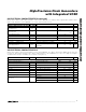
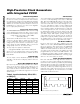
is always in high impedance. At the receiver end, the
two cables or PC board traces can be terminated as
shown in Figure 1.
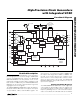
The VCXO output is divided down before driving the out-
put buffers. Program the dividing factor through the serial
interface. The MAX9450/MAX9451/MAX9452 feature two
output dividers DIV0 and DIV1 (see the Functional
Diagram). DIV0 drives OUT0 and either DIV0 or DIV1 can
drive OUT1. CR6[2] sets which divider output drives
OUT1. This function allows for programming OUT1 and
OUT0 to different frequencies.
Reference Clock Inputs
The MAX9450/MAX9451/MAX9452 feature two “any-
thing” differential clock inputs. “Anything” means that
the inputs take any differential signals, such as CML,
LVDS, LVPECL, or HSTL. The inputs can also take a
single-ended input. For example, with LVCMOS refer-
ence inputs, connect the inputs to the positive pins
INn+ and connect the negative pins INn- to a reference
voltage of V
DD
- 1.32V. See Figure 2.
Setting CR5[4] and CR6[3] selects the input reference.
Failure detection and revert function apply only to IN0
and IN1. Also, SEL0 and SEL1 or CR5[3:2] can disable
the corresponding inputs. See Table 2.
Frequency Selection and Programming
The output frequency at CLKn, (n = 0, 1) is determined by
the reference clock and the dividing factors M, Ni (i = 0, 1),
and P, shown in the following equation:
ff
M
Ni P
CLKn REF
=×
×
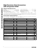
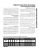
LVCMOS CLK OUTPUT
V
REF
= V
DD
- 1.32V
ANYTHING INPUT
Figure 2. Connecting LVCMOS Output to LVPECL Input
Z = 50Ω
LVPECL
OUTPUT
127Ω
127Ω
3.3V
83Ω
83Ω
LVPECL
INPUT
(A) LVPECL DC COUPLING
Z = 50Ω
HSTL
OUTPUT
50Ω
50Ω
HSTL
INPUT
(C) HSTL DC COUPLING
(B) LVDS COUPLING
Z = 50Ω
LVDS
OUTPUT
100Ω
LVDS
INPUT
Figure 1. DC LVPECL, LVDS, and HSTL Termination