
Owner manual


Note 1: All timing AC electrical characteristics and timing specifications are guaranteed by design and not production tested.
Note 2: The VCXO tracks the input clock frequency by ±50ppm.
Note 3: A master device must provide a hold time of at least 300ns for the SDA signal to bridge the undefined regions of SCL’s
falling edge.
Note 4: C
B
= total capacitance of one bus line in pF. Tested with C
B
= 400pF.
Note 5: Input filters on SDA and SCL suppress noise spikes less than 50ns.
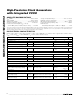
PARAMETER
SYMBOL
CONDITIONS
MIN TYP MAX
UNITS
Serial-Clock Frequency f
SCL
2
MHz
CS Fall to CLK Rise Setup Time t
CSS
12.5
ns
DIN Setup Time t
DS
12.5
ns
DIN Hold Time t
DH
0ns
CLK High to CS High t
CSH
0ns
CS Pulse-High Time t
CSW
20 ns
SERIAL SPI INTERFACE TIMING CHARACTERISTICS
(V
DD
= 2.4V to 3.6V, T
A
= -40°C to +85°C. See Figure 7 for the timing parameters definition.)
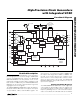
MAX9450/MAX9451/MAX9452
High-Precision Clock Generators
with Integrated VCXO
4 _______________________________________________________________________________________
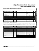
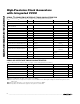
PARAMETER
SYMBOL
CONDITIONS
MIN TYP MAX
UNITS
Serial Clock f
SCL
400
kHz
Bus Free Time Between STOP and
START Conditions
t
BUF
1.3 µs
Rep eated H ol d Ti m e S TART C ond i ti on
t
HD
,
STA
0.6 µs
Rep eated S TART C ond i ti on S etup Ti m et
SU
,
STA
0.6 µs
STOP Condition Setup Time
t
SU
,
STO
0.6 µs
Data Hold Time
t
HD
,
DAT
(Note 3) 100 ns
Data Setup Time
t
SU
,
DAT
100 ns
SCL Clock-Low Period t
LOW
1.3 µs
SCL Clock-High Period t
HIGH
0.7 µs
Maximum Receive SCL/SDA Rise Time
t
R
300 ns
Minimum Receive SCL/SDA Rise Time
t
R
(Note 4)
20
+ 0.1 x C
b
ns
Maximum Receive SCL/SDA Fall Time
t
F
300 ns
Minimum Receive SCL/SDA Fall Time t
F
(Note 4)
20
+ 0.1 x C
b
ns
Fall Time of SDA, Transmitting t
F,TX
(Note 4)
20
+ 0.1C
b
250 ns
Pulse Width of Suppressed Spike t
SP
(Note 5) 0 50 ns
Capacitive Load for Each Bus Line C
B
(Note 4) 400 pF
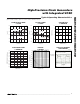
SERIAL I
2
C-COMPATIBLE INTERFACE TIMING CHARACTERISTICS
(V
DD
= 2.4V to 3.6V, T
A
= -40°C to +85°C. See Figure 4 for the timing parameters definition.)