
Owner manual
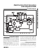


MAX9450/MAX9451/MAX9452
High-Precision Clock Generators
with Integrated VCXO
_______________________________________________________________________________________ 3
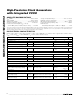
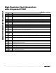
DC ELECTRICAL CHARACTERISTICS (continued)
(V
DDA
= V
DD
= V
DDQ
= 2.4V to 3.6V, and V
DDQ
= 1.4V to 1.6V for MAX9451, T
A
= -40°C to +85°C. Typical values at V
DDA
= V
DD
=
V
DDQ
= 3.3V, and V
DDQ
= 1.5V for MAX9451, T
A
= +25°C, unless otherwise noted.)
PARAMETER
SYMBOL
CONDITIONS
MIN
TYP
MAX
UNITS
SERIAL INTERFACE INPUT, OUTPUT (SCL, SDA, CS)
Input High Level V
IH
0.7
x V
DD
V
Input Low Level V
IL
0.3
x V
DD
V
Input Leakage Current I
IL
±1 µA
Output Low Level V
OL
3mA sink current 0.4 V
Input Capacitance C
I
10 pF
POWER CONSUMPTION
V
DD
and V
DDA
Supply Current I
CC1
Output clock frequency = 155MHz 55 85 mA
V
DDQ
Supply Current I
CC2
Output clock frequency = 155MHz
(MAX9450)
55 80 mA
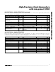
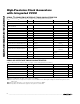
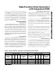
AC ELECTRICAL CHARACTERISTICS
(V
DDA
= V
DD
= V
DDQ
= 2.4V to 3.6V, and V
DDQ
= 1.4V to 1.6V for MAX9451, T
A
= -40°C to +85°C. |V
ID
| = 200mV, V
COM
= |V
ID
/ 2| to
2.4 - |V
ID
/ 2|. Typical values at V
DDA
= V
DD
= V
DDQ
= 3.3V and V
DDQ
= 1.5V for MAX9451, T
A
= +25°C. C
L
= 10pF, clock output =
155.5MHz and clock input = 19.44MHz, unless otherwise noted.) (Note 1)
PARAMETER
SYMBOL
CONDITIONS
MIN TYP MAX
UNITS
CLK OUTPUTS (CLK0, CLK1)
Reference Input Frequency f
IN
Measured at IN0 or IN1
0.008
500
MHz
Output Frequency f
OUT
Measured at CLK0 or CLK1 15 160
MHz
VCXO Pulling Range C
L
= 8pF (Note 2) ±50
ppm
Output-to-Output Skew t
SKO
Skew between CLK0 and CLK1 90 ps
Rise Time t
R
20% to 80% of output swing 0.4
0.585
ns
Fall Time t
F
80% to 20% of output swing 0.4
0.585
ns
Duty Cycle 44 56 %
Period Jitter (RMS) T
J
Measured at the band 12kHz to 20MHz
0.8 ps
1kHz offset -70
dBc/Hz
10kHz offset
-110
dBc/Hz
Phase Noise
100kHz offset
-130
dBc/Hz