
Owner manual


MAX9450/MAX9451/MAX9452
High-Precision Clock Generators
with Integrated VCXO
12 ______________________________________________________________________________________
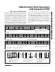
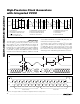
SMBCLK
AB CD
E
FG H
I
J
K
SMBDATA
t
SU:STA
t
HD:STA
t
LOW
t
HIGH
t
SU:DAT
t
HD:DAT
t
SU:STO
t
BUF
A = START CONDITION
B = MSB OF ADDRESS CLOCKED INTO SLAVE
C = LSB OF ADDRESS CLOCKED INTO SLAVE
D = R/W BIT CLOCKED INTO SLAVE
E = SLAVE PULLS SMBDATA LINE LOW
L
M
F = ACKNOWLEDGE BIT CLOCKED INTO MASTER
G = MSB OF DATA CLOCKED INTO MASTER
H = LSB OF DATA CLOCKED INTO MASTER
I = MASTER PULLS DATA LINE LOW
J = ACKNOWLEDGE CLOCKED INTO SLAVE
K = ACKNOWLEDGE CLOCK PULSE
L = STOP CONDITION
M = NEW START CONDITION
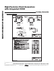
Figure 6. SMBus Read Timing Diagram
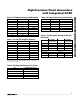
t
CSS
t
CSH
f
SCL
t
CSW
CS
SCLK
DIN
t
DS
t
DS
D0D1D14D15
Figure 7. SPI Write Operation Timing Diagram
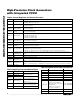
SLK
SDA
D15
D14
D13 D12
D11 D10
D9
D8
D7 D6
D5 D4
D3
D2 D1
D0
REGISTER ADDRESS
REGISTER DATA
CS
Figure 8. SPI Register Address and Data Configuration Function Setting Tables
SPI Interface
The SPI interface is activated when AD0 = AD1 = high.
The SPI port is a write-only interface, and it uses the
three inputs: CS, SCL, and SDA. Bit D15 is always 0,
indicating the write-only mode, as shown in Figure 5.
D14–D8 are the register address bits and D7–D0 are
the data bits. In Table 4, the register address mapping
is still valid, except the first address bit on the left is not
used. D14 is the LSB of the address, and D7 is the LSB
of the data. D15–D0 are sent with LSB (D15) first. The
maximum SCL frequency is 2MHz.
To perform a write, set D15 = 0, drive CS low, toggle
SCL to latch SDA data on the rising edge, then drive
CS high after 16 SCL cycles for two SCL cycles to sig-
nal the boundary of a 16-bit word (Figure 5). SCL must
be low when CS falls at the start of a transmission.
Switching of SCL and SDA is ignored unless CS is low.