
User guide
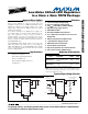

MAX8902A/MAX8902B
Low-Noise 500mA LDO Regulators
in a 2mm x 2mm TDFN Package
2 _______________________________________________________________________________________
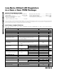
ABSOLUTE MAXIMUM RATINGS
Stresses beyond those listed under “Absolute Maximum Ratings” may cause permanent damage to the device. These are stress ratings only, and functional
operation of the device at these or any other conditions beyond those indicated in the operational sections of the specifications is not implied. Exposure to
absolute maximum rating conditions for extended periods may affect device reliability.
BYP, EN, IN, OUT, SELA, SELB, POK to GND, GS to GND, FB,
OUTS to GND .....................................................-0.3V to +6.0V
Output Short-Circuit Duration.....................................Continuous
Continuous Power Dissipation (T
A
= +70°C)
8-Pin, 2mm x 2mm TDFN
(derate 11.9mW/°C above +70°C).............................953.5mW
Operating Temperature Range .........................-40°C to +125°C
Junction Temperature Range ............................-40°C to +150°C
Storage Temperature Range .............................-65°C to +150°C
Lead Temperature (soldering, 10s) .................................+300°C
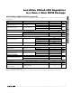
ELECTRICAL CHARACTERISTICS
(V
IN
= V
EN
= 5V, OUTS = OUT, circuit of Figure 2 (MAX8902A) and Figure 3 (MAX8902B), T
A
= -40°C to +125°C, unless otherwise
noted.) (Note 1)
PARAMETER CONDITIONS MIN TYP MAX UNITS
IN
Input Voltage Range 1.7 5.5 V
Input Undervoltage Lockout V
IN
rising, 100mV typical hysteresis 1.5 1.6 1.7 V
OUT
Output Voltage Range V
IN
≥ V
OUT
+ 0.1V 0.6 5.3 V
Output Voltage Accuracy
V
IN
= 1.7V to 5.5V for V
OUT
≤ 1.4V,
V
IN
= (V
OUT
+ 0.3V) to 5.5V for V
OUT
> 1.4V,
I
OUT
= 0.1mA to 500mA
-1.5 +1.5 %
Load Regulation I
OUT
= 0.1mA to 500mA 0.02 %
Line Regulation
V
IN
= 1.7V to 5.5V for V
OUT
≤ 1.4V,
V
IN
= (V
OUT
+ 0.3V) to 5.5V for V
OUT
> 1.4V,
I
OUT
= 200mA
0.04 %
V
IN
≥ 3.6V, T
A
≤ +85°C 50 100
V
IN
≥ 3.6V, T
A
≤ +125°C 120
Dropout Voltage
(Note 2)
I
OUT
= 500mA
V
IN
= 1.7V 150
mV
Current Limit V
OUT
= 95% of regulation, V
IN
= V
OUT
+ 0.5V 600 700 800 mA
Output Noise I
OUT
= 100mA, f = 10Hz to 100kHz, C
BYP
= 0.01µF 16 µV
RMS
f = 5kHz 92
f = 10kHz 85Power-Supply Rejection Ratio I
OUT
= 10mA
f = 100kHz 62
dB
OUTS (MAX8902A only)
OUTS Input Bias Current In regulation 0.5 7.0 µA
FB (MAX8902B only)
FB Threshold Accuracy V
IN
= 1.7V to 5.5V, I
OUT
= 0.1mA to 500mA 0.591 0.600 0.609 V
T
A
= +25°C -0.1 0.02 +0.1
FB Input Bias Current V
FB
= 0.6V
T
A
= -40°C 0.03
µA
BYP
BYP Capacitor Range Regulator remains stable 1 100 nF
BYP Startup Current From BYP to GND during startup 50 µA