
Manual
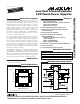

MAX8710/MAX8711/MAX8712
Low-Cost Linear-Regulator
LCD Panel Power Supplies
_______________________________________________________________________________________ 9
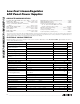
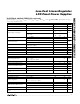
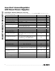
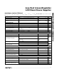
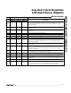
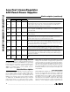
PIN
NAME
MAX8710 MAX8711 MAX8712
FUNCTION
GON
1——
Internal High-Voltage MOSFET Switch Common Terminal. GON is the output of the
high-voltage switch-control block. GON is internally pulled to GND by a 1kΩ
resistor in shutdown.
DRN
2——
Switch Input. Drain of the internal high-voltage back-to-back P-channel MOSFETs
connected to GON.
REF 3 1 1
Reference Output. Connect a 0.22µF capacitor from REF to GND. REF remains on
in shutdown.
POSB
42—Operational-Amplifier Noninverting Input
INL 5 3 2 Linear-Regulator Supply Input
NEGB
64—Operational-Amplifier Inverting Input
IN 7 5 3 IC Supply Input. Bypass IN to GND with a 0.1µF capacitor.
OUTL
864
Linear-Regulator Output. OUTL is internally pulled to GND by a 1kΩ resistor in
shutdown. For the MAX8711/MAX8712, OUTL is also the supply input for the
charge-pump regulators.
SUPCP
9——
Supply Input for the Charge-Pump Regulators. Connect a 0.1µF capacitor from
SUPCP to GND.
DRVN
10 7 5
Negative Charge-Pump Driver Output. Output high level is V
SUPCP
, and output
low level is GND. DRVN is internally pulled high to SUPCP when the negative
charge pump is disabled.
DRVP
11 8 6
Positive Charge-Pump Driver Output. Output high level is V
SUPCP
, and output low
level is GND. DRVP is internally pulled low in shutdown.
N. C.
12 — — No Connect. Not internally connected.
GND
13 9 7 Ground
OUTB
14 10 —
Operational-Amplifier Output. OUTB is internally pulled to GND by a 1kΩ resistor
in shutdown.
SUPB
15 11 —
Operational-Amplifier Supply Input. Bypass SUPB to GND with a 0.1µF capacitor.
THR
16 — —
GON Low-Level Regulation Set-Point Input. Connect THR to the center of a
resistive voltage-divider between REF and GND to set the V
GON
regulation level.
The actual level is 10 × V
THR
. See the Switch Control section for details.
Pin Description