
Manual

MAX8710/MAX8711/MAX8712
Low-Cost Linear-Regulator
LCD Panel Power Supplies
20 ______________________________________________________________________________________
Charge-Pump Regulators
Number of Charge-Pump Stages
For highest efficiency, always choose the lowest num-
ber of charge-pump stages that meets the output
requirement.
The number of positive charge-pump stages is given by:
where n
POS
is the number of positive charge-pump
stages, V
P
is the positive charge-pump regulator out-
put, V
INPUT
is the supply voltage for the charge-pump
regulators (V
SUPCP
, MAX8710 or V
OUTL
, MAX8711/
MAX8712), V
DIODE
is the forward-voltage drop of the
charge-pump diode, and V
SWITCH
is the voltage drop
of the internal switches. Use V
SWITCH
= 0.3V.
The number of negative charge-pump stages is given by:
where n
NEG
is the number of negative charge-pump
stages and V
GOFF
is the negative charge-pump regula-
tor output.
The above equations are derived based on the
assumption that the first stage of the positive charge
pump is connected to V
MAIN
and the first stage of the
negative charge pump is connected to ground.
Sometimes fractional stages are more desirable for bet-
ter efficiency. This can be done by connecting the first
stage to another available supply, such as a 5V supply.
If the first charge-pump stage is powered from 5V, then
the above equations become:
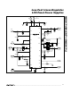
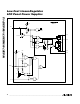
Output Voltage Selection
Adjust the positive charge-pump-regulator output volt-
age by connecting a resistive voltage-divider from the
regulator output V
P
to GND with the center tap connect-
ed to FBP (Figure 1). Select the lower resistor of divider
R4 in the range of 10kΩ to 50kΩ. Calculate upper resistor
R3 with the following equation:
where V
FBP
= 2.5V (typ) is the regulation point of the
positive charge-pump regulator.
Adjust the negative charge-pump-regulator output volt-
age by connecting a resistive voltage-divider from the
negative charge-pump output V
GOFF
to REF with the
center tap connected to FBN (Figure 1). Select R6 in
the 20kΩ to 100kΩ range. Calculate R5 with the follow-
ing equation:
where V
REF
= 5V and V
FBN
= 250mV is the regulation
point of the negative charge-pump regulator.
Flying Capacitor
Increasing the flying-capacitor (C
X
) value lowers the
effective source impedance and increases the output-
current capability of the charge pump. Increasing the
capacitance indefinitely has a negligible effect on out-
put-current capability because the internal switch resis-
tance and the diode impedance place a lower limit on
the source impedance. A 0.1µF ceramic capacitor
works well in most low-current applications. The flying
capacitor’s voltage rating must exceed the following:
V
CX
> n x V
INPUT
where n is the stage number in which the flying capaci-
tor is used, and V
INPUT
is the supply voltage for the
charge-pump regulators (V
SUPCP
, MAX8710 or V
OUTL
,
MAX8711/MAX8712).
Charge-Pump Input Capacitor
Use an input capacitor with a value equal to or greater
than the flying capacitor. Place the capacitor as close
to the IC as possible. Connect the capacitor directly
to PGND.
RR
VV
VV
FBN GOFF
REF FBN
56
=×
−
−
RR
V
V
P
FBP
34 1 =×
−
n
VV V
VV
n
VV V
VV
POS
PSWITCH
INPUT DIODE
NEG
GOFF SWITCH
INPUT DIODE
=
+
×
=
++
×
−
−
−
−
5
2
5
2
n
VV
VV
NEG
GOFF SWITCH
INPUT DIODE
=
+
×
−
−
2
n
VV V
VV
POS
PSWITCH SUPCP
INPUT DIODE
=
+
×
−
−
2