
Manual
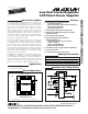

MAX8710/MAX8711/MAX8712
Low-Cost Linear-Regulator
LCD Panel Power Supplies
2 _______________________________________________________________________________________
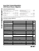
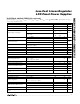
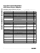
ABSOLUTE MAXIMUM RATINGS
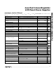
ELECTRICAL CHARACTERISTICS
(Circuit of Figure 1. V
IN
= V
INL
= V
SUPCP
= 12V, V
OUTL
= V
SUPB
= 10V, V
SRC
= 27V, T
A
= 0°C to +85°C. Typical values are at T
A
=
+25°C, unless otherwise noted.)
Stresses beyond those listed under “Absolute Maximum Ratings” may cause permanent damage to the device. These are stress ratings only, and functional
operation of the device at these or any other conditions beyond those indicated in the operational sections of the specifications is not implied. Exposure to
absolute maximum rating conditions for extended periods may affect device reliability.
CTL, FBL, FBP, FBN, SHDN, REF, THR to GND ......-0.3V to +6V
MODE, DLP to GND ....................................-0.3V to V
REF
+ 0.3V
IN, INL, OUTL (MAX8710) to GND.........................-0.3V to +28V
SUPCP, SUPB , OUTL (MAX8711, MAX8712)
to GND................................................................-0.3V to +14V
POSB, OUTB, NEGB to GND ....................-0.3V to V
SUPB
+ 0.3V
DRVN, DRVP to GND ..............................-0.3V to V
SUPCP
+ 0.3V
SRC to GND ...........................................................-0.3V to +30V
GON, DRN to GND......................................-0.3V to V
SRC
+ 0.3V
DRN to GON............................................................-30V to +30V
OUTB Maximum Continuous Output Current....................±75mA
DRVP RMS Output Current .................................................90mA
DRVN RMS Output Current..............................................-150mA
Continuous Power Dissipation (T
A
= +70°C)
24-, 16-, and 12-Pin Thin QFN 4mm x 4mm
(derate 16.9mW/°C above +70°C).............................1349mW
Operating Temperature Range .........................-40°C to +100°C
Junction Temperature......................................................+150°C
Storage Temperature Range .............................-65°C to +160°C
Lead Temperature (soldering, 10s) .................................+300°C
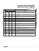
PARAMETER CONDITIONS
MIN TYP MAX
UNITS
IN Operating Supply Range 8 28 V
SHDN = GND 0.2 0.4
IN Quiescent Current
SHDN = 3.3V 2.5
mA
Duration to Trigger Fault Condition 2
16
oscillator clock cycles 44 ms
REF Output Voltage -10µA < I
REF
< 1mA (excluding internal load) 4.9 5.0 5.1 V
SUPCP Input Supply Range 2.7
13.2
V
Charge-Pump Regulators Operating
Frequency
1275 1500 1725
kHz
Thermal Shutdown Rising temperature, 15°C hysteresis
+160
°C
LINEAR REGULATOR
INL Operation Supply Range V
OUTL
< V
INL
728V
Dropout Voltage I
OUTL
= 50mA
150
300 mV
FBL Regulation Voltage I
OUTL
= 50mA
2.46 2.50 2.54
V
FBL Input Bias Current V
FBL
= 2.5V 50 nA
FBL Fault Trip Level Falling edge
1.92 2.00 2.08
V
V
INL
= V
IN
= 10.8V~13.2V, V
OUTL
= 10V,
I
OUTL
= 50mA
15
FBL Line-Regulation Error
V
INL
= V
IN
= 10V~28V, V
OUTL
= 9V, I
OUTL
= 50mA 10
mV
Bandwidth Guaranteed by design
1000
kHz
Maximum OUTL Current V
FBL
= 2.4V
300
mA
OUTL Soft-Start Period 2
12
oscillator clock cycles in a 7-bit DAC 3 ms
OUTL Load Regulation V
IN
= 12V, 5mA < I
OUTL
< 300mA 2 %
OPERATIONAL AMPLIFIER
SUPB Supply Operating Range 4.5
13.2
V
SUPB Supply Current Buffer configuration, V
POSB
= 4V, no load 0.7 1.0 mA
Input Offset Voltage (V
NEGB
, V
POSB
) = V
SUPB
/ 2, T
A
= +25°C012mV
Input Bias Current (V
NEGB
, V
POSB
) = V
SUPB
/ 2 -50 +1
+50
nA