
Owner manual


MAX7393/MAX7394
Precision Silicon Oscillators with
Enable or Autoenable
_______________________________________________________________________________________ 5
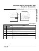
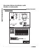
Pin Description
PIN
MAX7393 MAX7394
NAME FUNCTION
11V
CC
Positive Supply Voltage Input. Bypass V
CC
to GND with 0.1µF capacitors placed as close to
the device as possible. Connect V
CC
to V
CC2
.
2 2 GND Ground
3 3 I.C.
Internally Connected. Connect I.C. to GND. Do not connect I.C. to any other input or output.
Do not leave I.C. unconnected.
4 — CLKIN
Clock Input. Connect CLKIN to a returned clock signal source (see the Autoenable (CLKIN,
MAX7393) section).
5 5 CLOCK Clock Output. CLOCK is a rail-to-rail, push-pull output.
66V
CC2
Positive Supply Voltage Input for Output Driver. Bypass V
CC2
to GND with a 0.1µF capacitor
placed as close to the device as possible. Connect V
CC2
to V
CC
.
— 4 ENABLE
Enable Input. Drive ENABLE low to place the MAX7394 in shutdown mode. Drive ENABLE
high for normal operation.
——EP
Exposed Paddle, TDFN Version Only. Connect EP to ground. Do not connect EP to any other
input or output.
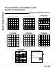
MAX7394 SETTLING TIME FROM START
MAX7393 toc09
CLOCK
2V/div
ENABLE
2V/div
400µs/div
CLOCK OUTPUT WAVEFORM
WITH C
L
= 10pF
MAX7393 toc10
CLOCK
1V/div
10ns/div
Typical Operating Characteristics (continued)
(V
CC
= V
CC2
= 3.3V, T
A
= +25°C, MAX7394, 48MHz output, unless otherwise noted.)