
User Manual


Depending on the command, byte 1 through byte N
may assume different functions. They may either be a
direct command (write, read, read all, reset), or an
address or data contents. The commands available in
the MAX7057 SPI are described in detail below:
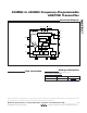
Write: The write command (0x01) is used to program
the MAX7057 registers (see Tables 2 and 3). The for-
mat shown in Figure 3 must be followed, allowing all the
registers to be programmed within one CS cycle.
Using a byte descriptive notation, the write command
can be viewed as the following sequence:
Data 0 is then written to the register addressed by
<Initial Address>, Data 1 is written to <Initial Address +
1>, and so on.
Read: To execute an SPI read operation, the general-
purpose output (GPO) pin must be configured to either
a CKOUT_SDO or SDO function (see Tables 15 and 16
for details).
SDI: <0x01> <Initial Address> <Data 0> <Data 1> … <Data N>
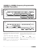
MAX7057
300MHz to 450MHz Frequency-Programmable
ASK/FSK Transmitter
______________________________________________________________________________________ 11
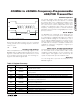
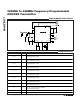
Figure 2. SPI Format
SDI
SCLK
CS
WRITE COMMAND (0x01) INITIAL ADDRESS (A[7:0]) DATA 0 DATA N
D7 D7D6 D5 D4 D3 D2 D1 D0A7 A6 A5 A4 A3 A2 A1 A0 D0
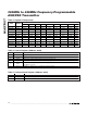
SDI
DATA 1 DATA N
SCLK
D7 D6 D5 D4 D3 D2 D1 D0 D7 D6 D5 D4 D3 D2 D1 D0
CS
Figure 3. SPI Write Command Format