
Manual
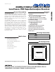


MAX7042
308MHz/315MHz/418MHz/433.92MHz
Low-Power, FSK Superheterodyne Receiver
8 _______________________________________________________________________________________
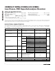
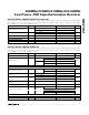
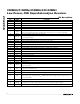
Pin Description
PIN NAME FUNCTION
1, 2 N.C. No Connection. Internally pulled down.
3, 25, 32
N.C. No Connection. Not internally connected.
4 RSSI Buffered Received-Signal-Strength-Indicator Output
5 XTAL2 Crystal Input 2. XTAL2 can be driven from an AC-coupled external reference.
6 XTAL1 Crystal Input 1. Bypass to GND if XTAL2 is driven by an AC-coupled external reference.
7AV
DD
Analog Power-Supply Voltage. AV
DD
is connected to an on-chip +3.0V regulator in +5V operation.
Bypass AV
DD
to GND with 0.1µF and 220pF capacitors placed as close to the pin as possible.
8 LNAIN Low-Noise Amplifier Input. Must be AC-coupled.
9
LNASRC
Low-Noise Amplifier Source for External Inductive Degeneration. Connect an inductor to GND to set
the LNA input impedance.
10
LNAOUT
Low-Noise Amplifier Output. Connect to AV
DD
through a parallel LC tank filter. AC-couple to MIXIN+.
11 MIXIN+ Noninverting Mixer Input. Must be AC-coupled to the LNA output.
12 MIXIN- Inverting Mixer Input. Bypass to AV
DD
or AGND with a capacitor.
13 MIXOUT 330Ω Mixer Output. Connect to the input of the 10.7MHz IF filter.
14 AGND Analog Ground
15 IFIN- Inverting 330Ω IF Limiter Amplifier Input. Bypass to AGND with a capacitor.
16 IFIN+ Noninverting 330Ω IF Limiter Amplifier Input. Connect to the output of the 10.7MHz IF filter.
17 PDMIN Minimum-Level Peak Detector for Demodulator Output
18 PDMAX Maximum-Level Peak Detector for Demodulator Output
19 DS- Inverting Data-Slicer Input
20 DS+ Noninverting Data-Slicer Input
21 OP+ Noninverting Op-Amp Input for the Sallen-Key Data Filter
22 DF Data-Filter Feedback Node. Input for the feedback of the Sallen-Key data filter.
23 DGND Digital Ground
24 DV
DD
Digital Power-Supply Voltage. Bypass to DGND with 0.01µF and 220pF capacitors placed as close to
the pin as possible.
26 EN
Enable. Internally pulled down. Drive high for normal operation. Drive low or leave unconnected to put
the device into shutdown mode.
27 FSEL1 Frequency-Select Pin 1 (see Table 1). Internally pulled down. Connect to EN for logic-high operation.
28 FSEL2 Frequency-Select Pin 2 (see Table 1). Internally pulled down. Connect to EN for logic-high operation.
29 HV
IN
High-Voltage Supply Input. For +3V operation, connect HV
IN
to AV
DD
and DV
DD
. For +5V operation,
connect only HV
IN
to +5V. Bypass HV
IN
to AGND with 0.01µF and 220pF capacitors placed as close
to the pin as possible.
30 DATA Receiver Data Output
31 LNASEL
LNA Bias Current Select Pin. Internally pulled down. Set LNASEL to logic-low for low LNA current and
set LNASEL to logic-high for high LNA current. Connect to EN for logic-high operation.
EP GND Exposed Paddle. Connect to ground.