
Manual


MAX7042
308MHz/315MHz/418MHz/433.92MHz
Low-Power, FSK Superheterodyne Receiver
2 _______________________________________________________________________________________
ABSOLUTE MAXIMUM RATINGS
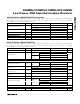
DC ELECTRICAL CHARACTERISTICS
(Typical Application Circuit, 50Ω system impedance, AV
DD
= DV
DD
= HV
IN
= +2.4V to +3.6V, f
RF
= 308, 315, 418, and 433.92MHz;
T
A
= -40°C to +125°C, unless otherwise noted. Typical values are at AV
DD
= DV
DD
= HV
IN
= +3.0V, f
RF
= 433.92MHz,
P
RFIN
≤ -80dBm, T
A
= +25°C, unless otherwise noted.)
Stresses beyond those listed under “Absolute Maximum Ratings” may cause permanent damage to the device. These are stress ratings only, and functional
operation of the device at these or any other conditions beyond those indicated in the operational sections of the specifications is not implied. Exposure to
absolute maximum rating conditions for extended periods may affect device reliability.
HV
IN
to AGND or DGND .......................................-0.3V to +6.0V
AV
DD
, DV
DD
to AGND or DGND..........................-0.3V to +4.0V
FSEL1, FSEL2, LNASEL,
EN, DATA...............................(DGND - 0.3V) to (HV
IN
+ 0.3V)
All Other Pins............................(AGND - 0.3V) to (AV
DD
+ 0.3V)
Continuous Power Dissipation (T
A
= +70°C)
32-Pin Thin QFN (derate 34.5mW/°C above +70°C)....2759mW
Operating Temperature Range .........................-40°C to +125°C
Storage Temperature Range .............................-65°C to +150°C
Maximum RF Input Power ................................................+0dBm
Lead Temperature (soldering, 10s) .................................+300°C
PARAMETER SYMBOL CONDITIONS MIN TYP MAX UNITS
Supply Voltage (3V) V
DD
HV
IN
, AV
DD
, and DV
DD
connected
to power supply
2.4 3.0 3.6 V
Supply Voltage (5V) HV
IN
HV
IN
connected to power supply,
AV
DD
and DV
DD
unconnected from
HV
IN
, but connected together
4.5 5.0 5.5 V
Operating, 1x I
LNA
6.2
315M H z ( 3V )
Operating, 2x I
LNA
6.8
Operating, 1x I
LNA
6.4
315M H z ( 5V )
Operating, 2x I
LNA
7.0
Operating, 1x I
LNA
6.4 8.7
434M H z ( 3V )
Operating, 2x I
LNA
7.0 8.6
Operating, 1x I
LNA
6.6 8.4
Supply Current I
DD
434M H z ( 5V )
Operating, 2x I
LNA
7.2 9.2
mA
T
A
= +25°C 0.02
T
A
= +85°C 0.1
Shutdown Current (3V) I
SHDN
All digital
inputs low
T
A
= +125°C 0.85 6
µA
T
A
= +25°C 0.6
T
A
= +85°C 1.4Shutdown Current (5V) I
SHDN
All digital
inputs low
T
A
= +125°C 4 7
µA
Startup Time t
ON
Time from EN = high to final signal
detection; does not include
baseband filter or data-
slicer reference settling
250 µs
DIGITAL I/O
Input High Threshold V
IH
0.9 x HV
IN
V
Input Low Threshold V
IL
0.1 x HV
IN
V