
Owner manual
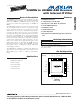

MAX7036
300MHz to 450MHz ASK Receiver
with Internal IF Filter
_______________________________________________________________________________________ 7
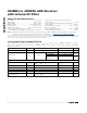
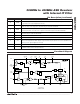
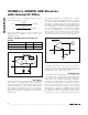
Functional Diagram
Pin Description (continued)
PIN NAME FUNCTION
13 DCOC
DC Offset Capacitor Connection. This is for the RSSI amplifier. Connect a 1µF capacitor from this pin
to ground (see the Typical Application Circuit).
14 OPP
Noninverting Op-Amp Input. This is for the Sallen-Key data filter. Connect a capacitor from this pin to
GND. The value of the capacitor is determined by the data-filter bandwidth.
15 DFFB
Data-Filter Feedback Input. Input for the feedback of the Sallen-Key data filter. Connect a capacitor
from this pin to DSP. The value of the capacitor is determined by the data-filter bandwidth.
16 DSP
Positive Data-Slicer Input. Connect a capacitor from this pin to DFFB. The value of the capacitor is
determined by the data-filter bandwidth.
17 DSN Negative Data-Slicer Input
18 PDOUT Peak-Detector Output
19 V
DD
Power-Supply Voltage Input. For 5.0V operation, V
DD
is the input to an on-chip voltage regulator
whose 3.2V output drives AVDD. Bypass to ground with a 0.1µF capacitor as close as possible to the
device (see the Typical Application Circuit).
20 DATAOUT Digital Baseband Data Output
—EP
Exposed Pad. Internally connected to ground. Connect to a large ground plane using multiple vias to
maximize thermal and electrical performance.
MAX7036
EP*
*EXPOSED PAD.
CONNECT TO GND.
3.2V
REGULATOR
PEAK
DETECTOR
REF
REF
∑
∑
AGC
DATAOUT DSN PDOUT DSP OPP DFFB
LNAOUT
MIXIN1
MIXIN2
XTAL1
XTAL2
ENABLE
V
DD
AVDD
DVDD
LNAIN
IFC1 IFC2 IFC3 DCOC
PLL
3
2
1
19
4
12
5
687 10 9 1311
20 17 18 16 14 15