
Instruction Manual


MAX6974/MAX6975
Data Segment
The bit length of the data segment received by the
MAX6974/MAX6975 is dependent on the command
specified in the header.
The load CALDAC command has three unique data
bytes, while load global-intensity PDM and load
configuration each have one byte of data repeated
three times. The CALDAC data within the command
load CALDAC is sent with B CALDAC data first, fol-
lowed by G CALDAC data, and then R CALDAC data,
as shown in Table 8.
The data segment of the load individual PWM command
has a variable length depending on specific device and
configuration settings. The data is always organized
as B driver data first in the order of B7 first to B0 last
(MSB first), followed by the G driver data in the same
order of G7 to G0 (MSB first), and then the R driver data
in the order of R7 to R0 (MSB first).
Tail Segment
The MAX6974/MAX6975 allow for an optional string of
data bits to be transmitted following all device data
bits, which is referred to as the tail segment. The data
bits of the tail segment are clocked back to the host,
following the header, from the last device in a cascaded
chain. The number of bits in the tail segment is optional.
The tail carries no device-specific data on DIN, but
provides feedback confirmation to the host that all data
bits were extracted by all devices in the cascade chain.
24-Output PWM LED Drivers
for Message Boards
18 ______________________________________________________________________________________
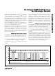
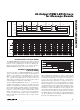
HEADER DATA 1 DATA 2 DATA 3 … DATA N
HDR[23:0] B[7:0] G[7:0] R[7:0] B[7:0] G[7:0] R[7:0] B[7:0] G[7:0] R[7:0] … B[7:0] G[7:0] R[7:0]
Table 8. Serial Format for Load CALDAC
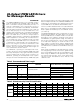
HEADER DATA 1 DATA 2 DATA 3 … DATA N
HDR[23:0] D[7:0] D[7:0] D[7:0] D[7:0] D[7:0] D[7:0] D[7:0] D[7:0] D[7:0] … D[7:0] D[7:0] D[7:0]
Table 9. Serial Format for Load Global-Intensity PDM
HEADER DATA 1 DATA 2 DATA 3 … DATA N
HDR[23:0] D[7:0] D[7:0] D[7:0] D[7:0] D[7:0] D[7:0] D[7:0] D[7:0] D[7:0] … D[7:0] D[7:0] D[7:0]
Table 10. Serial Format for Load Configuration
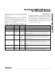
HEADER DATA 1 DATA 2 DATA 3 … DATA N
HDR[23:0] B7, B6, …R0 B7, B6, …R0 B7, B6, …R0 … B7…R0
Table 11. Serial Format for Load Individual PWM (Nonmultiplexed)
HEADER DATA 1 DATA 2 DATA 3 … DATA N
HDR[23:0] B7, B7', B6, B6', …R0' B7, B7', B6, B6', …R0' B7, B7', B6, B6', …R0' … B7, B7', B6, B6', …R0'
Table 12. Serial Format for Load Individual PWM (Multiplexed)
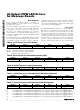
B[7:0] 8-bit data loaded into port B CALDAC
G[7:0] 8-bit data loaded into port G CALDAC
R[7:0] 8-bit data loaded into port R CALDAC
N Number of cascaded devices
D[7:0] Send the 8-bit data for the global-intensity PDM three times (24 total bits)
D[7:0] Send the 8-bit configuration data three times (24 total bits)
B_…G_…R_ 12-bit (MAX6974) or 14-bit (MAX6975) data each
B_ 12-bit (MAX6974) or 14-bit (MAX6975) PWM data for each output B_ during multiplex phase MUX0, MSB first
B_' 12-bit (MAX6974) or 14-bit (MAX6975) PWM data for each output B_ during multiplex phase MUX1, MSB first
G_ 12-bit (MAX6974) or 14-bit (MAX6975) PWM data for each output G_ during multiplex phase MUX0, MSB first
G_' 12-bit (MAX6974) or 14-bit (MAX6975) PWM data for each output G_ during multiplex phase MUX1, MSB first
R_ 12-bit (MAX6974) or 14-bit (MAX6975) PWM data for each output R_ during multiplex phase MUX0, MSB first
R_' 12-bit (MAX6974) or 14-bit (MAX6975) PWM data for each output R_ during multiplex phase MUX1, MSB first