
User guide


MAX6972/MAX6973
16-Output PWM LED Drivers
for Message Boards
_______________________________________________________________________________________ 5
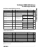
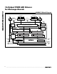
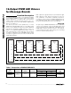
Pin Description
PIN NAME FUNCTION
1,17 V
DD
Positive Supply Voltage. Bypass V
DD
to GND with a 0.1µF ceramic capacitor.
2 MUX0 Multiplex 0 Active-Low, Open-Drain Output. Use MUX0 to drive a pnp transistor.
3 CLKI+ PWM and Serial-Interface Noninverting Clock LVDS Input
4 CLKI- PWM and Serial-Interface Inverting Clock LVDS Input
5 DIN+ Serial-Interface Noninverting Data LVDS Input
6 DIN- Serial-Interface Inverting Data LVDS Input
7 LOADI Serial-Interface Load CMOS Input
8 I.C. Internally Connected. Connect to GND.
9–16 Y0–Y7 Y LED Drive Outputs. Y0 to Y7 are open-drain, constant-current sinks.
18 LOADO Serial-Interface Load CMOS Output
19 DOUT- Serial-Interface Inverting Data LVDS Output
20 DOUT+ Serial-Interface Noninverting Data LVDS Output
21 CLKO- PWM and Serial-Interface Inverting Clock LVDS Output
22 CLKO+ PWM and Serial-Interface Noninverting Clock LVDS Output
23 MUX1 Multiplex 1 Active-Low, Open-Drain Output. Use MUX1 to drive a pnp transistor.
24 AGND Analog Ground. Connect to GND.
25–32 Z7–Z0 Z LED Drive Outputs. Z0 to Z7 are open-drain, constant-current sinks.
EP GND Power Ground. Exposed pad on package underside must be connected to GND.