
Owner manual


MAX6902
SPI-Compatible RTC in a TDFN
_______________________________________________________________________________________ 7
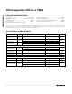
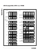
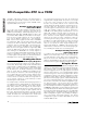
REGISTER ADDRESS REGISTER DEFINITION
FUNCTION A7 A6 A5 A4 A3 A2 A1 A0 VALUE D7 D6 D5 D4 D3 D2 D1 D0
RAM
RAM 0 RD 1 0 0 0 0 0 1 RAM DATA 0 xxxxxxxx
/W
••
••
••
••
••
••
RAM 30 RD 1 1 1 1 1 0 1 RAM DATA 30 xxxxxxxx
/W
RAM BURST RD 1111111
/W
Note: *POR STATE defines power-on reset state of register contents.
Figure 2. Register Address Definition (Sheet 3 of 3)
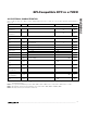
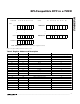
Table 2. Register Address and Description
WRITE (HEX) READ (HEX) DESCRIPTION POR CONTENTS (HEX)
01 81 Seconds 00
03 83 Minutes 00
05 85 Hours 00
07 87 Date 01
09 89 Month 01
0B 8B Day 01
0D 8D Year 70
0F 8F Control 00
13 93 Century 19
15 95 Alarm Configuration 00
17 97 Reserved 07
19 99 Seconds Alarm Threshold 7F
1B 9B Minutes Alarm Threshold 7F
1D 9D Hours Alarm Threshold BF
1F 9F Date Alarm Threshold 3F
21 A1 Month Alarm Threshold 1F
23 A3 Day Alarm Threshold 07
25 A5 Year Alarm Threshold FF
3F BF Clock Burst Not applicable