
User Manual
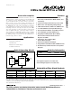
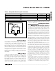


MAX6901
does not happen coincident with a Seconds counter
increment to ensure accurate time data is being read.
The clock counters continue to count and keep accu-
rate time during the Read operation.
The simplest way to read the timekeeping registers is to
use a Burst Read. In a Burst Read, the main timekeep-
ing registers (Seconds, Minutes, Hours, Date, Month,
Day, Year) and the Control register are read sequential-
ly in the order listed with the Seconds register first.
They are read out as a group of eight registers, with 8
bits each. All timekeeping registers (except Century)
are latched upon the receipt of the Burst Read com-
mand. The worst-case error between the “actual” time
and the “read” time is 1 second for a normal data transfer.
The timekeeping registers may also be read using
Single Reads. If Single Reads are used, it is necessary
to do some error checking on the receiving end,
because it is possible that the clock counters could
change during the Read operations, and report inaccu-
rate time data. The potential for error is when the
Seconds register increments before all the registers are
read. For example, suppose a carry of 13:59:59 to
14:00:00 occurs during Single Read operations. The
net data read could be 14:59:59, which is erroneous.
To prevent errors from occurring with Single Read oper-
ations, read the Seconds register first (initial-seconds)
and store this value for future comparison. After the
remaining timekeeping registers have been read,
reread the Seconds register (final-seconds). Check that
the final-seconds value equals the initial-seconds value;
if not, repeat the entire Single Read process. Using
Single Reads at a 100kHz serial speed, it takes under
2.5ms to read all seven of the timekeeping registers,
including two reads of the Seconds register.
Example: Reading the Clock
with a Burst Read
To read the time with a Burst Read, send BFh as the
Address/Command byte. Then clock out 8 bytes,
Seconds, Minutes, Hours, Date of the month, Month,
Day of the week, Year, and finally the Control byte. All
data are output LSB first. Decode the required informa-
tion based on the register definitions listed in Table 2.
Using the Alarm
A polled alarm function is available by reading the ALM
OUT bit. The ALM OUT bit is D7 of the Minutes time-
keeping register. A logic 1 in ALM OUT indicates the
alarm function is triggered. There are eight registers
associated with the alarm function, seven programma-
ble Alarm Threshold registers and one programmable
Alarm Configuration register. The Alarm Configuration
register determines which Alarm Threshold registers
are compared to the timekeeping registers, and the
ALM OUT bit sets if the compared registers are equal.
Table 2 shows the function of each bit of the Alarm
Configuration register. Placing a logic 1 in any given bit
of the Alarm Configuration register enables the respec-
3-Wire Serial RTC in a TDFN
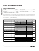
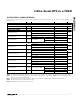
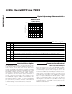
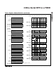
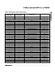
10 ______________________________________________________________________________________
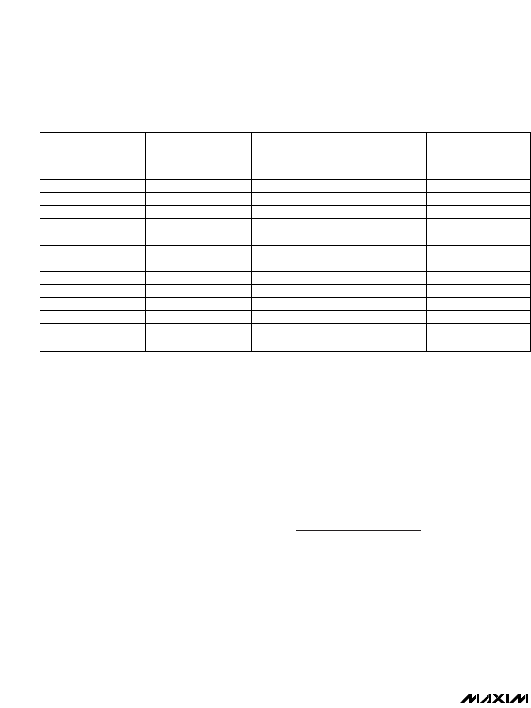
WRITE
ADDRESS/COMMAND
BYTE (HEX)
READ
ADDRESS/COMMAND
BYTE (HEX)
DESCRIPTION
POR CONTENTS
(HEX)
E4 E5 RAM 18 Indeterminate
E6 E7 RAM 19 Indeterminate
E8 E9 RAM 20 Indeterminate
EA EB RAM 21 Indeterminate
EC ED RAM 22 Indeterminate
EE EF RAM 23 Indeterminate
F0 F1 RAM 24 Indeterminate
F2 F3 RAM 25 Indeterminate
F4 F5 RAM 26 Indeterminate
F6 F7 RAM 27 Indeterminate
F8 F9 RAM 28 Indeterminate
FA FB RAM 29 Indeterminate
FC FD RAM 30 Indeterminate
FE FF RAM Burst Nonapplicable
Table 3. HEX Register Address/Description (continued)