
Owner's manual


MAX555
300Msps, 12-Bit DAC with
Complementary Voltage Outputs
_______________________________________________________________________________________ 5
_______________Detailed Description
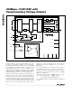
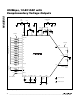
Figure 1’s functional diagram shows the MAX555’s three
major divisions: a digital section, a control-amplifier sec-
tion, and a resistor-divider network. The digital section
consists of a master/slave register, decoding logic, and
current switches. The control-amplifier section includes a
control amplifier and an array of 23 current sources divid-
ed into three groups. The resistor divider scales the cur-
rents from these groups to achieve the correct binary
weighting at the output. The output of the resistor-divider
network is laser trimmed to 50Ω, a key feature for driving
into controlled impedance transmission lines.
The first group of current sources comprises the six
MSBs, D11–D6 (resulting in 15 identical, plus two binary
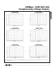
Pin Description
PIN NAME FUNCTION
1, 14, 16–19, 27,
28, 29, 31–38, 48,
49, 64
AGND
Analog Ground. Note: Exposed pad on the back of the package must be connected to
AGND.
2, 6, 54, 60 DGND Digital Ground
3 D8 Data Bit 8 (ECL Input)
4 D9 Data Bit 9 (ECL Input)
5 D10 Data Bit 10 (ECL Input)
7, 53 DV
EE
-5.2V Digital Power Supply
8 D11 Data Bit 11 (ECL Input)—MSB
9, 10, 11, 13, 39,
46, 58
N.C. No Connection
12 LBIAS Ladder-Bias Alternate Compensation Output. Connect bypass capacitor to AV
EE
.
15
ALTCOMPC
Control-Amplifier PTAT Reference Compensation Input. Connect bypass capacitor to AV
EE
.
20 ROFFSET Offset Compensation Input
21, 22 REF Analog Reference Voltage Inputs (Kelvin Connection)
23 REF/2 Analog Reference Voltage Center-Tap Input
24, 25 AV
EE
-5.2V Analog Power Supply
26
LOOPCRNT
Test Node. Must connect to AGND.
30
ALTCOMPIB
PTAT-IB Reference Compensation Output. Connects bypass capacitor to AV
EE
.
40, 41 VOUT Complementary DAC Output
42, 43 LGND Ladder Ground
44, 45 VOUT DAC Output
47 D0 Data Bit 0 (ECL Input)—LSB
50 D1 Data Bit 1 (ECL Input)
51 D2 Data Bit 2 (ECL Input)
52 D3 Data Bit 3 (ECL Input)
55 CLK Complementary Clock Input (ECL Input)
56 CLK Clock Input (ECL Input)
57 BYPASS Disables Latching of Data when High (ECL Input)
59 D4 Data Bit 4 (ECL Input)
61 D5 Data Bit 5 (ECL Input)
62 D6 Data Bit 6 (ECL Input)
63 D7 Data Bit 7 (ECL Input)