
Owner's manual


MAX555
300Msps, 12-Bit DAC with
Complementary Voltage Outputs
_______________________________________________________________________________________ 3
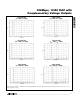
ELECTRICAL CHARACTERISTICS (continued)
(AV
EE
= DV
EE
= -5.2V, V
REF
= 1.000V, T
MIN
to T
MAX
= 0°C to +70°C, unless otherwise noted.) (Note 2.)
AV
EE
= DV
EE
= -5.2V
AV
EE
= DV
EE
= -5.2V
V
IL
= -1.95V
VOUT, VOUT
VOUT, VOUT
V
IH
= -0.75V
V
REF
= 1.000V, R
L
= 0Ω
T
A
= +25°C
T
A
= +25°C
Bypass = 1, transparent mode (Notes 4, 7)
Bypass = 1, transparent mode (Notes 4, 7)
-3dB
V
REF
= 1.000V
Bypass = 0, clocked mode (Notes 4, 7)
Bypass = 0, clocked mode (Notes 4, 7)
Bypass = 0, clocked mode (Notes 4, 7)
Bypass = 1, transparent mode (Notes 4, 7)
CONDITIONS
mA110 150 190DI
EE
Digital Power-Supply Current
mA30 46 60AI
EE
Analog Power-Supply Current
pF15C
OUT
Output Capacitance
Ω49.5 50.0 50.5R
OUT
Output Resistance
mA19.0 20.0 21.0I
OUT
Full-Scale Output Current
µV-250 0 +250V
OS
Input Offset Voltage
kV/V320AV
OL
Open-Loop Gain
MHz10BWMultiplying Input Bandwidth
Ω775 800 825R
IN
Amplifier Input Resistance
ps900t
DD
MSBs Decode Delay
µA12I
IL
Input Current, Logic Low
µA10 200I
IH
Input Current, Logic High
ns2.9t
PD1
MSBs Data-to-VOUT
Propagation Delay
ns2t
PD2
LSBs Data-to-VOUT
Propagation Delay
ns2.8t
PD3
Clock-to-VOUT
Propagation Delay
ns0.8t
HOLD
Data-to-Clock Hold Time
V-1.1 -0.75 0V
IH
Logic "1" Voltage
V-2.0 -1.95 -1.48V
IL
Logic "0" Voltage
ns1t
SU
Data-to-Clock Setup Time
UNITSMIN TYP MAXSYMBOLPARAMETER
W0.98 1.3P
DISS
Power Dissipation
°C/W25T
JA
Package Thermal Resistance,
Junction to Ambient
Note 2: All devices are 100% production tested at +25°C and are guaranteed by design for T
A
= T
MIN
to T
MAX
as specified.
Note 3: The gain-error method of calculation is shown below:
Definition:
[V
MEASURE(FS)
- V
IDEAL(FS)
] x 100
GE(%) = ––––––––––––––––––––––––––––––––––
V
IDEAL(FS)
where FS indicates full-scale measurements.
GE Method:
GE(%) = [(4096 / 4095) V
MEASURE
- 16(V
REF
/ R
IN
) (R
OUT
)] x 100
–––––––––––––––––––––––––––––––––––––––––––––——
16(V
REF
/ R
IN
) (R
OUT
)
= [(4096 / 4095) V
MEASURE
- 1] x 100
––––––––––––––––––––––––––––––––
1
where: V
REF
= 1.000V, R
IN
= 800Ω, R
OUT
= 50Ω, V
MEASURE
= VOUT (FS).
Note 4: Dynamic and timing specifications are obtained from device characterization and simulation testing and are not production tested.
Note 5: Spurious-free dynamic range is measured from the fundamental frequency to any harmonic or nonharmonic spurs within the
bandwidth f
CLK
/2, unless otherwise specified.
Note 6: Guaranteed by design.
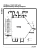
Note 7: Timing definitions are detailed in Figure 2.
Minimum data rate = DC (Note 6) MHz300f
D
Data Update Rate
DIGITAL INPUTS
CONTROL AMPLIFIER
OUTPUT PERFORMANCE
POWER SUPPLIES
DIGITAL TIMING