
Manual

MAX5440
Stereo Volume Control
with Rotary Encoder Interface
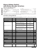
ABSOLUTE MAXIMUM RATINGS
Stresses beyond those listed under “Absolute Maximum Ratings” may cause permanent damage to the device. These are stress ratings only, and functional
operation of the device at these or any other conditions beyond those indicated in the operational sections of the specifications is not implied. Exposure to
absolute maximum rating conditions for extended periods may affect device reliability.
SHDN, MUTE, RENCODEA, RENCODEB,
and MODE to GND............................-0.3V to (V
LOGIC
+ 0.3V)
H_, L_, and W_ to V
SS
...............................-0.3V to (V
DD
+ 0.3V)
LEDIND_, MODEIND to GND................-0.3V to (V
LOGIC
+ 0.3V)
MIDBIAS, BIAS to V
SS
......................(V
SS
- 0.3V) to (V
DD
+ 0.3V)
V
LOGIC
to GND...........................................-0.3V to (V
DD
+ 0.3V)
V
DD
to GND..............................................................-0.3V to +6V
V
DD
to V
SS
................................................................-0.3V to +6V
V
SS
to GND...............................................................-3V to +0.3V
Input and Output Latchup Immunity...............................±200mA
Continuous Power Dissipation (T
A
= +70°C)
24-Pin SSOP (derate 8mW/°C above +70°C) ..............640mW
Operating Temperature Range ...........................-40°C to +85°C
Junction Temperature......................................................+150°C
Storage Temperature Range .............................-60°C to +150°C
Lead Temperature (soldering, 10s) .................................+300°C
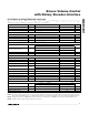
ELECTRICAL CHARACTERISTICS
(V
DD
= +2.7V to +5.5V, V
SS
= GND = 0, 2.7V ≤ (V
DD
- V
SS
) ≤ 5.5V, V
LOGIC
= +2.7V to V
DD
, V
H_
= V
DD
, V
L_
= V
DD
/ 2, T
A
= T
MIN
to
T
MAX
, unless otherwise specified. Typical values are at T
A
= +25°C.) (Note 1)
2 _______________________________________________________________________________________
PARAMETER SYMBOL CONDITIONS MIN TYP MAX UNITS
End-to-End Resistance R 36 40 52 kΩ
Absolute Tolerance ±0.25 dB
Tap-to-Tap Tolerance ±0.1 dB
V
H _
= ( V
D D
/ 2) + 1V
RM S
, 1kH z tap at top , R
L
= ∞ to V
L_
= V
D D
/ 2, 20H z to 20kH z
0.004
V
H _
= ( V
D D
/ 2) + 1.5V
RM S
, 1kH z tap at top ,
R
L
= ∞ to V
L_
= V
D D
/ 2, 20H z to 20kH z
0.006
V
DD
= 5V,V
SS
= 0V, V
L_
= 1.5V, V
H_
=
(V
DD
/ 2) + 1V
RMS
, 1kHz tap at top, R
L
=
10kΩ to V
MIDBIAS
, 20Hz to 20kHz
0.004
Total Harmonic Distortion Plus
Noise
THD+N
V
DD
= 5V,V
SS
= 0V, V
L_
= 5V, V
H _
= ( V
D D
/
2) + 1.5V
RM S ,
1kHz tap at top, R
L
= 10kΩ
to V
MIDBIAS
, 20Hz to 20kHz
0.006
%
Channel Isolation 100 dB
Interchannel Matching ±0.5 dB
Mute Attenuation SHDN = V
DD
90 dB
Power-Supply Rejection Ratio PSRR Input referred, 217Hz, 100mV
P-P
on V
DD
-60 dB
H Terminal Capacitance C
H
5pF
L Terminal Capacitance C
L
7pF
End-to-End Resistance
35 ppm/°C
Ratiometric Resistance
5 ppm/°C
Bandwidth, -3dB f
CUTOFF
C
W
= 33pF 100 kHz
Output Noise e
n
20Hz to 20kHz 3.2 µV
RMS
WIPER BUFFER
Output Voltage Swing V
O
R
L
= 10kΩ to V
MIDBIAS
V
DD
- 0.2 V
Output Current 3mA
Output Resistance R
OWB
110Ω
DC Offset -5 ±2 +5 mV
INTEGRATED BIAS GENERATOR
Output Voltage I
LOAD
= 1mA
(V
DD
+
V
SS
) / 2
- 10mV
(V
DD
+
V
SS
)
/ 2
( V
D D
+
V
S S
) / 2 +
10m V
V