
Manual


MAX5406
Audio Processor with Pushbutton Interface
2 _______________________________________________________________________________________
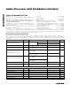
ABSOLUTE MAXIMUM RATINGS
Stresses beyond those listed under “Absolute Maximum Ratings” may cause permanent damage to the device. These are stress ratings only, and functional
operation of the device at these or any other conditions beyond those indicated in the operational sections of the specifications is not implied. Exposure to
absolute maximum rating conditions for extended periods may affect device reliability.
L1_H, L1_L, L2_H, L2_L
to V
SS
.......................-0.3V to the lower of (V
DD
+ 0.3V) or +6V
R1_H, R1_L, R2_H, R2_L
to V
SS
.......................-0.3V to the lower of (V
DD
+ 0.3V) or +6V
AMB, BALL, BALR, VOLUP, VOLDN, MUTE, SHDN, BASSDN,
BASSUP, TREBDN, TREBUP
to DGND .............-0.3V to the lower of (V
LOGIC
+ 0.3V) or +6V
CTL_, CTR_, CBL_, CBR_, CLS_, CRS_, CSUB, CBIAS, CMSNS,
AMBLI, AMBRI, BIAS
to V
SS
.......................-0.3V to the lower of (V
DD
+ 0.3V) or +6V
LOUT, ROUT, SUBOUT, LMR,
LPR to V
SS
................-0.3V to the lower of (V
DD
+ 0.3V) or +6V
V
DD
to V
SS
................................................................-0.3V to +6V
V
DD
to V
LOGIC
........................................................................±6V
V
LOGIC
to DGND ......................................................-0.3V to +6V
DGND to V
SS
............................................................-0.3V to +6V
LOUT, ROUT, SUBOUT Short Circuited to V
SS
.........Continuous
Continuous Power Dissipation (T
A
= +70°C)
48-Pin TQFN (derate 27.8mW/°C above +70°C) ........2222mW
48-Pin TSSOP (derate 16mW/°C above +70°C) .........1282mW
Operating Temperature Range ...........................-40°C to +85°C
Junction Temperature......................................................+150°C
Storage Temperature Range .............................-60°C to +150°C
Lead Temperature (soldering, 10s) .................................+300°C
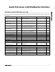
ELECTRICAL CHARACTERISTICS
(V
DD
= V
LOGIC
= +5.0V, V
SS
= 0, V
BIAS
= V
CMSNS
= V
DD
/ 2, DGND = 0, ambience disabled, V
AMBLI
= V
AMBRI
= V
BIAS,
V
R1_L
=
V
L1_L
= V
R2_L
= V
L2_L
= external V
BIAS
, C
CSUB
= 0.15µF, C
CLS
= C
CRS
= 1µF, C
CBL
= C
CBR
= 3.3nF, C
CTL
= C
CTR
= 4.7nF, C
BIAS
=
0.1µF, C
CBIAS
= 50µF (see the Typical Application Circuit), T
A
= T
MIN
to T
MAX
unless otherwise specified. Typical values are at T
A
=
+25°C). (Note1)
PARAMETER
SYMBOL
CONDITIONS
MIN TYP MAX
UNITS
R
INH
810
Signal-Inputs Input Resistance R
IN
With respect to
V
BIAS
R
INL
16 20
kΩ
Signal-Inputs Input Capacitance C
IN
With respect to V
BIAS
5pF
RF Rejection
2MHz to 2.4GHz two-tone test, 2/2.01MHz
input to 10kHz out
20 dBc
V
DD
= +5V, V
SS
= 0, V
CM
= V
BIAS
, gain
error ≤ -0.5dB
-4 +4
Differential Input Voltage Range V
IN
V
DD
= +2.7V, V
SS
= -2.7V, V
CM
= V
BIAS
,
gain error ≤ -0.5dB
-4.5 +4.5
V
V
DD
= +5V, V
SS
= 0, V
BIAS
= V
DD
/ 2,
V
DIFF
= 100mV
Common-Mode Input Voltage Range
V
CM
V
DD
= +2.7V, V
SS
= -2.7V, V
BIAS
= 0,
V
DIFF
= 100mV
V
SS
+ 0.5V V
DD
- 0.5V
V
Bias Voltage V
BIAS
Internally generated (V
CMSNS
= V
SS
)(V
DD
+ V
SS
) / 2 V
Bias-Voltage Input Current
L_ _H
=
R_ _H
=
V
BIAS,
L_ _L = R_ _L =
open, V
CMSNS =
V
DD
1mA
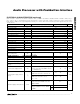
AUDIO PROCESSING FUNCTIONS
Maximum Balance Difference (Note 2) 10 12 14 dB
Minimum Balance Difference (Note 2) 0 dB
Balance Resolution (Note 2) 2 dB
Maximum Volume Attenuation (Note 2) -63 -62 -59 dB
Minimum Volume Attenuation (Note 2)
-0.5
0
+0.5
dB
Volume Resolution (Note 2) 2 dB
Volume-Control Steps (Note 2) 32
steps