
Instruction Manual

MAX4399
Audio/Video Switch for Three SCART
Connectors
_______________________________________________________________________________________ 5
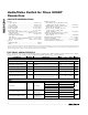
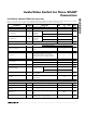
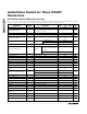
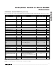
ELECTRICAL CHARACTERISTICS (continued)
(V
V12
= 12V, V
V_VID
= 5V, V
V_DIG
= 5V, 0.47µF X5R capacitor in parallel with a 10µF aluminum electrolytic capacitor from V_AUD to
G_AUD, no load, T
A
= 0°C to +70°C, unless otherwise noted. Typical values are at T
A
= +25°C.) (Note 1)
PARAMETER SYMBOL CONDITIONS MIN TYP MAX UNITS
Minimum Receive SCL/SDA Rise
Time (Note 3)
t
R
20 +
0.1C
B
ns
Maximum Receive SCL/SDA Fall
Time (Note 3)
t
F
300 ns
Minimum Receive SCL/SDA Fall
Time (Note 3)
t
F
20 +
0.1C
B
ns
Setup Time for Stop Condition t
SU
,
STO
0.6 µs
Bus Free Time Between a Stop
and Start
t
BUF
1.3 µs
OTHER DIGITAL PINS
DEV_ADDR Low Level 0.8 V
DEV_ADDR High Level 2.6 V
INTERRUPT_OUT Low Voltage INTERRUPT_OUT sinking 1mA 0.15 0.4 V
INTERRUPT_OUT High Leakage
Current
V
INTERRUPT_OUT
= 5V 1 10 µA
SLOW SWITCHING
Input Low Level 02V
Input Medium Level 4.5 7.0 V
Input High Level 9.5 12.0 V
Input Current 50 100 µA
Output Low Level R
LOAD
= 10kΩ to ground 0 1.5 V
Output Medium Level (External
16/9)
R
LOAD
= 10kΩ to ground 5.0 6.5 V
Output High Level (External 4/3) R
LOAD
= 10kΩ to ground 10 12 V
FAST SWITCHING
Input Low Level 0 0.4 V
Input High Level 13V
Input Current 110µA
Output Low Level I
SINK
= 0.5mA 0 0.01 0.2 V
Output High Level V_VID - V
OH
, I
SOURCE
= 20mA 0.75 2 V
Fast-Switching Output to RGB
Skew
Difference in propagation delays of fast-
switching signal and RGB signals;
measured from 50% input transition to 50%
output transition
30 ns
Fast-Switching Output Rise Time R
LOAD
= 150Ω to ground 30 ns
Fast-Switching Output Fall Time R
LOAD
= 150Ω to ground 30 ns
Note 1: All devices are 100% tested at T
A
= +25°C. All temperature limits are guaranteed by design.
Note 2: Parameter guaranteed by design.
Note 3: C
B
= total capacitance of one bus line in pF. Tested with C
B
= 400pF.