
Instruction Manual
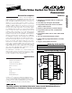

MAX4399
Audio/Video Switch for Three SCART
Connectors
4 _______________________________________________________________________________________
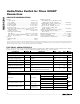
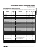
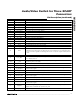
ELECTRICAL CHARACTERISTICS (continued)
(V
V12
= 12V, V
V_VID
= 5V, V
V_DIG
= 5V, 0.47µF X5R capacitor in parallel with a 10µF aluminum electrolytic capacitor from V_AUD to
G_AUD, no load, T
A
= 0°C to +70°C, unless otherwise noted. Typical values are at T
A
= +25°C.) (Note 1)
PARAMETER SYMBOL CONDITIONS MIN TYP MAX UNITS
Input DC Level Gain = 0dB V_AUD/2 V
Input Signal Amplitude
Inferred through total harmonic distortion
specification, f = 1kHz
2V
RMS
Input Resistance 100 kΩ
Output DC Level V_AUD/2 V
Signal-to-Noise Ratio SNR
f = 1.0kHz, 1V
RMS
, gain = 0dB, 20Hz to
20kHz
105 dB
f = 1.0kHz, 0.5V
RMS
0.002
Total Harmonic Distortion THD R
LOAD
= 10kΩ
f = 1.0kHz, 2V
RMS
0.005
%
Output Impedance 0.5 Ω
TV audio, volume control
range extends from -56dB
to +6dB
1.5 2 2.5
Volume Attenuation Step
1.414V
P-P
input
VCR, AUX audio 5.5 6 6.5
dB
Power-Supply Rejection Ratio PSRR f = 1kHz, 0.5V
P-P
110 dB
Mute Suppression f = 1kHz, 0.5V
RMS
input 105 dB
Audio Limiter Level f = 1kHz, 2.5V
RMS
input 6.7 V
P-P
Crosstalk f = 1kHz, 0.5V
RMS
, gain = 0dB 105 dB
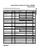
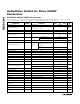
DIGITAL INTERFACE: SDA and SCL
Low-Level Input Voltage V
IL
0.8 V
High-Level Input Voltage V
IH
2.6 V
Hysteresis of Schmitt Trigger
Input
0.2 V
I
SINK
= 3mA 0 0.4
SDA Low-Level Output Voltage V
OL
I
SINK
= 6mA 0 0.6
V
Output Fall Time for SDA Line 400pF bus load 250 ns
Spike Suppression 50 ns
Input Current V
IL
= 0V, V
IH
= 5V -10 +10 µA
Input Capacitance 5pF
SCL Clock Frequency 0 400 kHz
Hold Time t
HD
,
STA
Repeated start condition 0.6 µs
Low Period of SCL Clock t
LOW
1.3 µs
High Period of SCL Clock t
HIGH
0.6 µs
Setup Time for a Repeated Start
Condition
t
SU,STA
0.6 µs
Data Hold Time t
HD
,
DAT
0 0.9 µs
Data Setup Time t
SU
,
DAT
100 ns
Maximum Receive SCL/SDA Rise
Time
t
R
(Note 3) 300 ns