
Instruction Manual

_______________Detailed Description
The MAX4198/MAX4199 are precision low-power differ-
ential amplifiers with factory-trimmed internal gain-set-
ting resistors. The MAX4198 is trimmed to a gain of
+1V/V and the MAX4199 is trimmed to a gain of +10V/V.
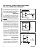
Input Stage
The
Functional Diagram
shows the internal structure of
the MAX4198/MAX4199. Although the resistors are pre-
cision matched, their absolute value varies by ±25%.
The typical input impedance for the MAX4198 is 50kΩ
for the noninverting input and 25kΩ for the inverting
input. The typical input impedance for the MAX4199 is
275kΩ for the noninverting input and 25kΩ for the
inverting input.
The common-mode inputs of the internal op amp can
range from V
EE
to (V
CC
- 1.1V). Although the inputs to
the internal op amp are not rail-to-rail, the internal resis-
tors form a voltage divider that extends the input com-
mon-mode range beyond-the-rails for the MAX4198.
The overall input range of the MAX4198 extends 100mV
beyond-the-rails without adversely affecting common-
mode rejection or undergoing phase reversal (V
CC
=
5V). The MAX4199 input common-mode range extends
from 100mV below the negative rail to (V
CC
- 1V) (see
the Input Common-Mode Voltage Range vs. Supply
Voltage graph in the
Typical Operating Characteristics
).
MAX4198/MAX4199
Micropower, Single-Supply, Rail-to-Rail
Precision Differential Amplifiers
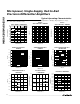
_______________________________________________________________________________________ 9
-0.5
1.5
0.5
4.5
3.5
2.5
7.5
6.5
5.5
243 5678
MAX4199
INPUT COMMON-MODE RANGE vs.
SUPPLY VOLTAGE
MAX4198toc28
SUPPLY VOLTAGE (V)
INPUT COMMON-MODE VOLTAGE (V)
V
REF
= V
CC
/2
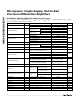
Typical Operating Characteristics (continued)
(V
CC
= +5V, V
EE
= 0V, R
L
= 25kΩ to V
CC
/ 2, V
SHDN
= V
CC
- 1.5V, small-signal V
OUT
= 100mVp-p, large-signal V
OUT
= 1Vp-p,
T
A
= +25°C, unless otherwise noted.)
-0.5
1.5
0.5
4.5
3.5
2.5
7.5
6.5
5.5
8.5
243 5678
MAX4198
INPUT COMMON-MODE RANGE vs.
SUPPLY VOLTAGE
MAX4198toc29
SUPPLY VOLTAGE (V)
INPUT COMMON-MODE VOLTAGE (V)
V
REF
= V
CC
/2
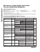
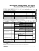
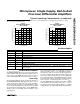
Pin Description
Feedback Resistor. Can be used as a sense input.FB5
Amplifier OutputOUT6
Positive Supply VoltageV
CC
7
Shutdown Control. Shutdown threshold is referenced to V
CC
. When pulled 2.5V below V
CC
, part
is in shutdown.
SHDN
8
Negative Supply VoltageV
EE
4
Noninverting InputIN+3
PIN
Inverting InputIN-2
Reference Voltage Input. Offsets output voltage.REF1
FUNCTIONNAME