
Instruction Manual

MAX4198/MAX4199
Micropower, Single-Supply, Rail-to-Rail
Precision Differential Amplifiers
2 _______________________________________________________________________________________
ABSOLUTE MAXIMUM RATINGS
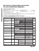
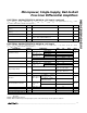
ELECTRICAL CHARACTERISTICS—MAX4198 (+5V Supply)
(V
CC
= +5V, V
EE
= 0V, R
L
= 25kΩ tied to V
CC
/ 2, V
REF
= V
CC
/ 2, V
SHDN
= V
CC
- 1.5V, typical values are at T
A
= +25°C,
T
A
= T
MIN
to T
MAX
, unless otherwise noted.) (Note 1)
Stresses beyond those listed under “Absolute Maximum Ratings” may cause permanent damage to the device. These are stress ratings only, and functional
operation of the device at these or any other conditions beyond those indicated in the operational sections of the specifications is not implied. Exposure to
absolute maximum rating conditions for extended periods may affect device reliability.
Supply Voltage (V
CC
to V
EE
)..................................................+8V
All Other Pins to GND ......................(V
EE
- 0.3V) to (V
CC
+ 0.3V)
Output Short Circuit Duration (to V
CC
or V
EE
)............Continuous
Continuous Power Dissipation (T
A
= +70°C)
SO (derate 9.09mW/°C above +70°C)..........................471mW
µMAX (derate 4.1mW/°C above +70°C) .......................330mW
Operating Temperature Range ...........................-40°C to +85°C
Junction Temperature......................................................+150°C
Storage Temperature Range............................ -65°C to +150°C
Lead Temperature (soldering, 10sec).............................+300°C
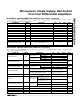
V
EE
+ 0.1V ≤
V
OUT
≤ V
CC
-
0.1V
Sink/source
R
L
= 5kΩ, ±10mV input overdrive
R
L
= 25kΩ, ±10mV input overdrive
f = 0.1Hz to 10Hz
f = 10kHz
V
CM
= V
EE
- 0.1V
to V
CC
+ 0.1V
f = 100Hz
f = 10Hz
Common-mode
IN- differential-mode
MAX4198ESA
MAX4198EUA
IN+ differential-mode
+2.7V ≤ V
CC
≤ +7.5V, V
CM
= +1.5V,
V
REF
= +1.5V, R
L
= 25kΩ to +1.5V
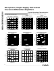
CONDITIONS
Gain Temperature Coefficient ppm/°C
±0.2 ±3
±0.01 ±0.1
mA±5.5Short-Circuit Current
V
EE
+ 0.2 V
EE
+ 0.1 to
to V
CC
- 0.2 V
CC
- 0.1
Output Voltage Swing V
V
EE
+ 0.1 V
EE
+ 0.03 to
to V
CC
- 0.1 V
CC
- 0.03
µV
RMS
7.8
Input Noise Voltage
nV√Hz
58
60
120
dB90 115PSRPower-Supply Rejection
±1.35 ±3.75
2.7 7.5
dB
74 90
CMR
DC
DC Common-Mode Rejection
kΩ
50
R
IN
25
Input Resistance
VV
CC
Supply Voltage Range
(Note 2)
±0.5 ±5
µV/°C
±1 ±20
TCOInput Offset Voltage Drift
50
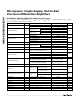
UNITSMIN TYP MAXSYMBOLPARAMETER
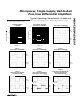
Single supply
Dual supply
Guaranteed by CMR test VV
EE
- 0.1 V
CC
+ 0.1V
IN
Input Voltage Range
V
CM
= V
EE
- 0.1 to V
CC
+ 0.1V,
f = 60Hz, f = 120Hz
dB90CMR
AC
AC Common-Mode Rejection
R
L
= 25kΩ, V
EE
+ 0.1V ≤
V
OUT
≤ V
CC
- 0.1V
V
CM
= V
CC
/ 2,
T
A
= +25°C
R
L
= 5kΩ, V
EE
+ 0.2V ≤
V
OUT
≤ V
CC
- 0.2V
%
±0.01 ±0.1
Gain Error
MAX4198ESA
±0.65 ±6MAX4198EUA
V
EE
+ 0.1V ≤ V
OUT
≤ V
CC
- 0.1VNonlinearity %±0.0003
70 90MAX4198EUA
MAX4198ESA
T
A
= +25°C,
V
CM
= V
CC
/ 2
T
A
= T
MIN
to T
MAX
,
V
CM
= V
CC
/ 2
±750
±100 ±1000
±30 ±500
µV
±2300
V
OS
Input Offset Voltage
MAX4198ESA
MAX4198EUA
MAX4198ESA
MAX4198EUA