
Manual

MAX4040–MAX4044
Single/Dual/Quad, Low-Cost, SOT23,
Micropower, Rail-to-Rail I/O Op Amps
_______________________________________________________________________________________ 9
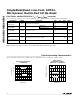
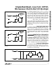
The MAX4040–MAX4044 family’s inputs are protected
from large differential input voltages by internal 2.2kΩ
series resistors and back-to-back triple-diode stacks
across the inputs (Figure 2). For differential input volt-
ages (much less than 1.8V), input resistance is typically
45MΩ. For differential input voltages greater than 1.8V,
input resistance is around 4.4kΩ, and the input bias
current can be approximated by the following equation:
I
BIAS
= (V
DIFF
- 1.8V) / 4.4kΩ
In the region where the differential input voltage
approaches 1.8V, the input resistance decreases expo-
nentially from 45MΩ to 4.4kΩ as the diode block begins
conducting. Conversely, the bias current increases with
the same curve.
Rail-to-Rail Output Stage
The MAX4040–MAX4044 output stage can drive up to a
25kΩ load and still swing to within 60mV of the rails.
Figure 3 shows the output voltage swing of a MAX4040
configured as a unity-gain buffer, powered from a single
+4.0V supply voltage. The output for this setup typically
swings from (V
EE
+ 10mV) to (V
CC
- 10mV) with a 100kΩ
load.
Applications Information
Power-Supply Considerations
The MAX4040–MAX4044 operate from a single +2.4V to
+5.5V supply (or dual ±1.2V to ±2.75V supplies) and
consume only 10µA of supply current per amplifier. A
high power-supply rejection ratio of 85dB allows the
amplifiers to be powered directly off a decaying battery
voltage, simplifying design and extending battery life.
Power-Up Settling Time
The MAX4040–MAX4044 typically require 200µs to
power up after V
CC
is stable. During this start-up time,
the output is indeterminant. The application circuit
should allow for this initial delay.
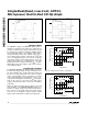
R3
R3 = R1 R2
R1 R2
MAX4040–
MAX4044
V
IN
Figure 1b. Minimizing Offset Error Due to Input Bias Current
(Inverting)
2.2k
2.2k
IN-
IN+
Figure 2. Input Protection Circuit
R3
V
IN
R3 = R1 R2
R1 R2
MAX4040–
MAX4044
Figure 1a. Minimizing Offset Error Due to Input Bias Current
(Noninverting)