
Manual
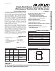
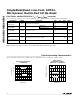

MAX4040–MAX4044
Single/Dual/Quad, Low-Cost, SOT23,
Micropower, Rail-to-Rail I/O Op Amps
2 _______________________________________________________________________________________
ABSOLUTE MAXIMUM RATINGS
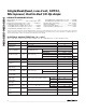
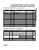
ELECTRICAL CHARACTERISTICS—T
A
= +25°C
(V
CC
= +5.0V, V
EE
= 0, V
CM
= 0, V
OUT
= V
CC
/ 2, SHDN = V
CC
, R
L
= 100kΩ tied to V
CC
/ 2, unless otherwise noted.)
Stresses beyond those listed under “Absolute Maximum Ratings” may cause permanent damage to the device. These are stress ratings only, and functional
operation of the device at these or any other conditions beyond those indicated in the operational sections of the specifications is not implied. Exposure to
absolute maximum rating conditions for extended periods may affect device reliability.
Supply Voltage (V
CC
to V
EE
)..................................................+6V
All Other Pins ...................................(V
CC
+ 0.3V) to (V
EE
- 0.3V)
Output Short-Circuit Duration to V
CC
or V
EE
..............Continuous
Continuous Power Dissipation (T
A
= +70°C)
5-Pin SOT23 (derate 7.1mW/°C above +70°C).............571mW
8-Pin µMAX (derate 4.1mW/°C above +70°C)..............330mW
8-Pin SO (derate 5.88mW/°C above +70°C).................471mW
10-Pin µMAX (derate 5.6mW/°C above +70°C)...........444mW
14-Pin SO (derate 8.33mW/°C above +70°C)..............667mW
Operating Temperature Range ...........................-40°C to +85°C
Junction Temperature......................................................+150°C
Storage Temperature Range.............................-65°C to +160°C
Lead Temperature (soldering, 10sec).............................+300°C
14 20V
CC
= 5.0V
V
EE
≤ V
CM
≤ V
CC
Input Offset Current I
OS
±0.5 ±3.0 nA
V
EE
≤ V
CM
≤ V
CC
V
IN+
- V
IN-
< 1.0V
Differential Input
Resistance
R
IN(DIFF)
45 MΩ
2.0 5.0
V
IN+
- V
IN-
> 2.5V
SHDN = V
EE
, MAX4041
and MAX4043 only
Large-Signal
Voltage Gain
Shutdown Supply
Current per Amplifier
I
CC(SHDN)
1.0
Supply-Voltage Range V
CC
2.4 5.5 VInferred from PSRR test
Output Voltage
Swing High
4.4 kΩ
V
OH
Inferred from the CMRR test
mV
A
VOL
dB
PARAMETER SYMBOL MIN TYP MAX UNITS
Supply Current
per Amplifier
I
CC
10
µA
94
V
CC
= 2.4V
10
Specified as
V
CC
- V
OH
Power-Supply
Rejection Ratio
PSRR dB
(V
EE
+ 0.2V) ≤ V
OUT
≤ (V
CC
- 0.2V)
60 90
74 85
Output Voltage
Swing Low
Input Common-Mode
Voltage Range
R
L
= 100kΩ
R
L
= 25kΩ
R
L
= 100kΩ
R
L
= 25kΩ
µA
V
CM
V
EE
V
CC
V
2.4V ≤ V
CC
≤ 5.5V 75 85
V
CC
= 2.4V
V
OL
mV
10
Specified as
V
EE
- V
OL
Input Bias Current I
B
±2 ±10 nA
40 60
R
L
= 100kΩ
R
L
= 25kΩ
Output Short-Circuit
Current
I
OUT(SC)
mA
0.7Sourcing
2.5
Channel-to-Channel
Isolation
Sinking
dB
CONDITIONS
80Specified at DC, MAX4042/MAX4043/MAX4044 only
V
CC
= 5.0V
±0.20 ±2.0
V
OS
Input Offset Voltage
mV
±0.25 ±2.5
V
EE
≤ V
CM
≤ V
CC
70 94
dBCMRR
Common-Mode
Rejection Ratio
MAX404_EU_
All other packages
65 94
V
EE
≤ V
CM
≤ V
CC
MAX4044ESD
MAX404_EU_
All other packages mV±0.20 ±1.50