
Owner manual


MAX3671
Low-Jitter Frequency Synthesizer
with Selectable Input Reference
_______________________________________________________________________________________ 3
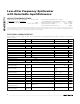
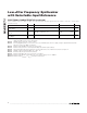
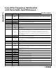
ELECTRICAL CHARACTERISTICS (continued)
(V
CC
= +3.0V to +3.6V, T
A
= -40°C to +85°C, C
PLL
= 0.1µF, C
REG
= 0.22µF. Typical values are at V
CC
= +3.3V, T
A
= +25°C, unless
otherwise noted.)
PARAMETER SYMBOL CONDITIONS MIN TYP MAX UNITS
REFERENCE CLOCK INPUTS (REFCLK0, REFCLK0, REFCLK1, REFCLK1)
Reference Clock Frequency f
REF
Table 1 MHz
Reference Clock Frequency
Tolerance
-200 +200 ppm
Reference Clock Duty Cycle 40 60 %
Reference Clock Amplitude
Detection Assert Threshold
V
DT
Differential swing (Notes 5, 6) 200 mV
P-P
LVPECL OUTPUTS (OUTA[3:0],
OUT
A
[3:0],
OUTB[4:0],
OUTB[4:0])
(Note 7)
Output High Voltage V
OH
V
CC
-
1.13
V
CC
-
0.98
V
CC
-
0.83
V
Output Low Voltage V
OL
V
CC
-
1.85
V
CC
-
1.70
V
CC
-
1.55
V
Differential-Output Swing 1.1 1.45 1.8 V
P-P
Output Current When Disabled V
O
= V
CC
- 2.0V to V
CC
- 0.7V 130 μA
Output Frequency f
OUT
Tables
2, 3
MHz
Output Rise/Fall Time t
R
, t
F
20% to 80% (Note 8) 150 500 ps
PLL_BYPASS = 0 48 52
Output Duty Cycle
PLL_BYPASS = 1 (Note 9) 45 55
%
Within output bank 20
Output-to-Output Skew t
SKEW
All outputs 40
ps
OTHER AC ELECTRICAL SPECIFICATIONS
PLL Jitter Transfer Bandwidth 40 kHz
Jitter Peaking 0.1 dB
PFD Compare Frequency 62.5 MHz
VCO Center Frequency 2.5 GHz
Random Jitter Generation Integrated 12kHz to 20MHz (Notes 5, 8) 0.3 1.0 ps
RMS
Determinisitic Jitter Caused by
Power-Supply Noise
(Note 10) 5 ps
P-P
Frequency Difference Between
Reference Clock and VCO
Within Which the PLL is
Considered in Lock
500 ppm
Frequency Difference Between
Reference Clock and VCO at
Which the PLL is Considered
Out-of-Lock
800 ppm
PLL Lock Time t
LOCK
Figure 2 600 μs