9-3275; Rev 1; 10/04 USB On-the-Go Transceiver and Charge Pump The MAX3301E fully integrated USB On-the-Go (OTG) transceiver and charge pump allows mobile devices such as PDAs, cellular phones, and digital cameras to interface directly with USB peripherals and each other without the need of a host PC. Use the MAX3301E with an embedded USB host to directly connect to peripherals such as printers or external hard drives.
MAX3301E USB On-the-Go Transceiver and Charge Pump ABSOLUTE MAXIMUM RATINGS All voltages are referenced to GND. VCC, VL .....................................................................-0.3V to +6V TRM (regulator off or supplied by VBUS) ..-0.3V to (VBUS + 0.3V) TRM (regulator supplied by VCC)...............-0.3V to (VCC + 0.3V) D+, D- (transmitter tri-stated) ...................................-0.3V to +6V D+, D- (transmitter functional)....................-0.3V to (VCC + 0.3V) VBUS ..................
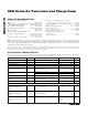
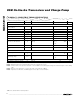
USB On-the-Go Transceiver and Charge Pump (VCC = +3V to +4.5V, VL = +1.65V to +3.6V, CFLYING = 100nF, CVBUS = 1µF, ESRCVBUS = 0.1Ω (max), TA = TMIN to TMAX, unless otherwise noted. Typical values are at VCC = +3.7V, VL = +2.5V, TA = +25°C.) (Note 2) PARAMETER OE/INT, SPD, SUS, RESET DAT_VP, SE0_VM Input Low Voltage SYMBOL CONDITIONS MIN TYP VIL ADD Input High Voltage VIHA ADD Input Low Voltage VILA MAX UNITS 0.
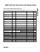
MAX3301E USB On-the-Go Transceiver and Charge Pump DC ELECTRICAL CHARACTERISTICS (continued) (VCC = +3V to +4.5V, VL = +1.65V to +3.6V, CFLYING = 100nF, CVBUS = 1µF, ESRCVBUS = 0.1Ω (max), TA = TMIN to TMAX, unless otherwise noted. Typical values are at VCC = +3.7V, VL = +2.5V, TA = +25°C.) (Note 2) PARAMETER Switching Frequency SYMBOL CONDITIONS MIN fSW TYP MAX 390 UNITS kHz VBUS Leakage Voltage vbus_drv = 0 0.2 V VBUS Rise Time CVBUS = 10µF, IVBUS = 8mA, measured from 0 to +4.
USB On-the-Go Transceiver and Charge Pump (VCC = +3V to +4.5V, VL = +1.65V to +3.6V, CFLYING = 100nF, CVBUS = 1µF, ESRCVBUS = 0.1Ω (max), TA = TMIN to TMAX, unless otherwise noted. Typical values are at VCC = +3.7V, VL = +2.5V, TA = +25°C.
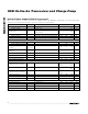
MAX3301E USB On-the-Go Transceiver and Charge Pump I2C-/SMBus™- COMPATIBLE TIMING SPECIFICATIONS (VCC = +3V to +4.5V, VL = +1.65V to +3.6V, CFLYING = 100nF, CVBUS = 1µF, ESRCVBUS = 0.1Ω (max), TA = TMIN to TMAX, unless otherwise noted. Typical values are at VCC = +3.7V, VL = +2.5V, TA = +25°C.) (Note 2) PARAMETER SYMBOL CONDITIONS MIN TYP MAX UNITS 400 kHz Serial Clock Frequency fSCL Bus-Free Time Between Stop and Start Conditions tBUF 1.3 µs Start-Condition Hold Time tHD_STA 0.
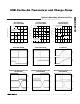
USB On-the-Go Transceiver and Charge Pump LINEAR REGULATOR POWERED BY VCC 30 20 10 VCC = 3.0V VCC = 4.2V 5.25 5.00 4.75 4.50 LINEAR REGULATOR POWERED BY VCC 4.00 0 4 8 12 16 20 5.50 5.25 IVBUS = 0 5.00 IVBUS = 8mA 4.75 LINEAR REGULATOR POWERED BY VCC 4.25 0 5.75 MAX3301E toc03 5.50 VBUS OUTPUT VOLTAGE (V) 40 VBUS OUTPUT VOLTAGE vs. INPUT VOLTAGE (VCC) MAX3301E toc02 VCC = 3.3V VCC = 4.2V VBUS OUTPUT VOLTAGE (V) INPUT CURRENT (ICC) (mA) 50 VBUS OUTPUT VOLTAGE vs.
Typical Operating Characteristics (continued) (Typical operating circuit, VCC = +3.7V, VL = +2.5V, CFLYING = 100nF, TA = +25°C, unless otherwise noted.) DRIVER PROPAGATION DELAY LOW-TO-HIGH (FULL-SPEED MODE) DRIVER ENABLE DELAY (FULL-SPEED MODE) MAX3301E toc10 MAX3301E toc11 MAX3301E toc12 OE/INT 1V/div DAT_VP 1V/div OE/INT 1V/div D+ 1V/div D+ 1V/div D1V/div D1V/div D+ 1V/div D1V/div 4ns/div 10ns/div 10ns/div DRIVER DISABLE DELAY (LOW-SPEED MODE) MAX3301E toc13 SUPPLY CURRENT vs.
USB On-the-Go Transceiver and Charge Pump PIN NAME FUNCTION THIN QFN UCSP 1, 4, 9, 12, 17, 25, 28 — N.C. 2 D2 DAT_VP 3, 29 D1, E3 VCC 5 C1 C- 6 C2 SE0_VM 7, 21 B1, C5 GND Ground 8 A1 SDA I2C-Compatible Serial Data Interface. Open-drain data input/output. 10 B2 SCL I2C-Compatible Serial Clock Input No Connection. Not internally connected. System-Side Data Input/Output. DAT_VP is an input if OE/INT is logic 0. DAT_VP is an output if OE/INT is logic 1.
MAX3301E USB On-the-Go Transceiver and Charge Pump Pin Description (continued) PIN NAME FUNCTION THIN QFN UCSP 20 C3 ADD I2C-Interface Address Selection Input. (See Table 5.) 22 C4 ID_IN ID Input. ID_IN is internally pulled up to VCC. The state of ID_IN determines ID bits 3 and 5 of the interrupt source register (see Table 10). 23 D5 D- USB Differential Data Input/Output. Connect D- to the D- terminal of the USB connector through a 27.4Ω ±1% series resistor.
USB On-the-Go Transceiver and Charge Pump 3V D+ tR tF VOH 90% 0V DtPHL tPLH VL RCV 10% VOL VL / 2 0V tPHL tPLH DAT_VP Figure 5. Rise and Fall Times VL VL / 2 0V DAT_VP tPLH tPHL tPHL SE0_VM tPLH VL VL / 2 0V SE0_VM D+/D- RISE/FALL TIMES ≤ 8ns, VL = 1.8V, 2.5V, OR 3.3V D+ VOHD VCRS_F, VCRS_L VCRS_F, VCRS_L Figure 9. D+/D- to RCV, DAT_VP, SE0_VM Propagation Delays (VP_VM Mode) D- VOLD Figure 6.
USB On-the-Go Transceiver and Charge Pump MAX3301E Block Diagram ID DETECTOR ADD INT RESET ID_IN C+ C- VBUS CHARGE PUMP SERIAL CONTROLLER SCL VBUS COMPARATORS VBUS LINEAR REGULATOR TRM PULLUP/PULLDOWN RESISTORS SDA CAR KIT INTERRUPT DETECTOR DAT_VP SE0_VM OE/INT VP VM RCV POWER BLOCK D- DIFF RX LEVEL TRANSLATOR VCC VL D+ DIFF TX SE D+ GND SPD SUS SE DMAX3301E Figure 11.
USB On-the-Go Transceiver and Charge Pump The USB OTG specification defines a dual-role USB device that acts either as an A device or as a B device. The A device supplies power on V BUS and initially serves as the USB host. The B device serves as the initial peripheral and requires circuitry to monitor and pulse VBUS. These initial roles can be reversed using HNP. The MAX3301E combines a low- and full-speed USB transceiver with additional circuitry required by a dualrole device.
MAX3301E USB On-the-Go Transceiver and Charge Pump ID_IN The USB OTG specification defines an ID input that determines which dual-role device is the default host. An OTG cable connects ID to ground in the connector of one end and is left unconnected in the other end. Whichever dual-role device receives the grounded end becomes the A device. The MAX3301E provides an internal pullup resistor on ID_IN. Internal comparators detect if ID_IN is grounded or left floating.
USB On-the-Go Transceiver and Charge Pump Data Transfer Transmitting Data to the USB The MAX3301E transceiver features two modes of transmission: DAT_SE0 or VP_VM (see Table 3). Set the transmitting mode with dat_se0 (bit 2 in control register 1, see Table 7). In DAT_SE0 mode with OE/INT low, DAT_VP specifies data for the differential transceiver, and SE0_VM forces D+/D- to the single-ended zero (SE0) state. In VP_VM mode with OE/INT low, DAT_VP drives D+, and SE0_VM drives D-.
MAX3301E USB On-the-Go Transceiver and Charge Pump General-Purpose Buffer Mode Set gp_en (bit 7 in special-function register 1) and dat_se0 (bit 2 in control register 1) to 1, set uart_en (bit 6 in control register 1) to zero, and drive OE/INT low to place the MAX3301E in general-purpose buffer mode. Control the direction of data transfer with dminus_dir and dplus_dir (bits 3 and 4 of special-function register 1, see Tables 2 and 14).
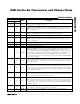
USB On-the-Go Transceiver and Charge Pump CONTROL PIN/BIT MODE INPUT OUTPUT DESCRIPTION DAT_SE0 DAT_VP SE0_VM D+ D- 0 OE/INT 0 1 0 0 0 1 0 0 1 1 0 1 0 0 0 0 1 0 1 0 0 0 0 0 1 1 1 0 0 0 0 0 0 0 0 0 0 0 0 0 0 1 0 1 0 0 0 0 0 0 1 0 1 0 0 0 0 1 1 1 1 1 0 0 1 0 0 0 1 1 0 0 1 1 0 1 0 1 0 0 1 0 1 0 0 1 0 0 1 1 1 0 0 1 0 0 0 0 0 0 0 1 0 0 0 1 0 1 0 1 0 0 0 0 1 0 1 1 0 0 0 1 1 1 1
MAX3301E USB On-the-Go Transceiver and Charge Pump Table 4.
USB On-the-Go Transceiver and Charge Pump MAX3301E waits for a START condition followed by its slave address. The LSB of the address word is the read/write (R/W) bit. R/W indicates whether the master is writing to or reading from the MAX3301E (R/W = 0 selects the write condition, R/W = 1 selects the read condition). After receiving the proper address, the MAX3301E issues an ACK. The MAX3301E has two possible addresses (see Table 5).
MAX3301E USB On-the-Go Transceiver and Charge Pump SLAVE ADDRESS (7 BITS) S A6 A5 A4 A3 A2 A1 SLAVE ADDRESS (7 BITS) RS A6 A5 A4 A3 A2 A1 A0 R/W A 0 0 A0 R/W A 1 0 REGISTER ADDRESS (8 BITS) A MSB LSB DATA (8 BITS) MSB LSB 0 NA P 1 0 Figure 19.
USB On-the-Go Transceiver and Charge Pump A6 A5 A4 A3 A2 R/W A1 A0 0 SLAVE ADDRESS (7 BITS) S A6 A5 A4 A3 A2 A0 DATA (K) (8 BITS) LSB DATA (K+3) (8 BITS) LSB MSB LSB SLAVE ADDRESS (7 BITS) A6 A5 A4 A3 A2 R/W A1 A0 SLAVE ADDRESS (7 BITS) S A6 A5 A4 A3 A2 0 A1 A0 1 A NA P LSB P LSB UNSUPPORTED REGISTER ADDRESS (K) (8 BITS) — ALL 0's RETURNED A DATA (K+N) (8 BITS) MAX3301E SENDS AN ACK MSB R/W LSB MSB UNSUPPORTED REGISTER ADDRESS (K) (8 BITS) A A MSB A M
MAX3301E USB On-the-Go Transceiver and Charge Pump Table 6. Register Map REGISTER MEMORY ADDRESS Vendor ID 00h, 01h Read only. The contents of registers 00h and 01h are 6Ah and 0Bh, respectively. DESCRIPTION Product ID 02h, 03h Read only. The contents of registers 02h and 03h are 01h and 33h, respectively. Control 1 04h (set) 05h (clear) Sets operating modes, maximum data rate, and direction of data transfer.
USB On-the-Go Transceiver and Charge Pump SYMBOL 0 speed Set to 0 for low-speed (1.5Mbps) mode. Set to 1 for full-speed (12Mbps) mode. This bit changes the data rate only if spd_susp_ctl = 1 in special-function register 1. 0 1 suspend Set to 0 for normal operating mode. Set to 1 for suspend mode. This bit changes the operating mode only if spd_susp_ctl = 1 in special-function register 1. 0 2 dat_se0 Set to 0 for VP_VM USB mode. Set to 1 for DAT_SE0 USB mode. 0 3 — Not used.
MAX3301E USB On-the-Go Transceiver and Charge Pump Table 9. VBUS Control Logic SET COMMAND (ADDRESS 06h) BEHAVIOR OF MAX3301E vbus_drv vbus_dischrg vbus_chrg vbus_drv vbus_dischrg vbus_chrg 1 X X 1 0 0 0 1 X 0 1 0 0 0 1 0 0 1 0 0 0 Not affected Not affected Not affected Table 10. Interrupt Source Register (Address 08h is Read Only) BIT NUMBER SYMBOL 0 vbus_vld Logic 1 if VBUS > VBUS valid comparator threshold.
USB On-the-Go Transceiver and Charge Pump CONTENTS VALUE AT POWER-UP BIT NUMBER SYMBOL 0 vbus_vld Set to 0 to disable the vbus_vld interrupt for a high-to-low transition. Set to 1 to enable the vbus_vld interrupt for a high-to-low transition. See Tables 10 and 11. 0 1 sess_vld Set to 0 to disable the sess_vld interrupt for a high-to-low transition. Set to 1 to enable the sess_vld interrupt for a high-to-low transition. See Tables 10 and 11.
MAX3301E USB On-the-Go Transceiver and Charge Pump Special-Function Registers Tables 14 and 15 describe the special-function registers. Special-function register 1 determines whether hardware or software controls the maximum data rate and suspend behavior, sets the direction of data transfer, and toggles general-purpose buffer mode.
USB On-the-Go Transceiver and Charge Pump 01h ESD Protection To protect the MAX3301E against ESD, D+, D-, ID_IN, and VBUS have extra protection against static electricity to protect the device up to ±15kV. The ESD structures withstand high ESD in all states; normal operation, suspend mode, interrupt shutdown, and shutdown. For the ESD structures to work correctly, connect a 1µF or greater capacitor from TRM to GND and from VBUS to GND.
RC 50MΩ to 100MΩ CHARGE-CURRENTLIMIT RESISTOR HIGHVOLTAGE DC SOURCE Cs 150pF IEC 61000-4-2 The IEC 61000-4-2 standard covers ESD testing and performance of finished equipment; it does not specifically refer to integrated circuits. The MAX3301E helps the user design equipment that meets level 3 of IEC 61000-4-2, without the need for additional ESD-protection components.
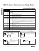
USB On-the-Go Transceiver and Charge Pump N.C. C+ VBUS VP VCC N.C. TRM VM N.C. TOP VIEW 32 31 30 29 28 27 26 25 1 MAX3301E 24 D+ SDA OE/INT RCV VL SUS GND SCL SPD INT RESET C- SE0_VM ADD ID_IN GND VCC DAT_VP VP VM D- C+ VBUS VCC TRM D+ 1 2 3 4 5 A DAT_VP 2 23 D- VCC 3 22 ID_IN N.C. 4 21 GND C- 5 20 ADD SE0_VM 6 19 RESET GND 7 18 INT SDA 8 17 N.C. MAX3301E 9 10 11 12 13 14 15 16 N.C. SCL OE/INT N.C.
USB On-the-Go Transceiver and Charge Pump MAX3301E Typical Operating Circuit VL VCC 1µF 0.1µF VL(I/O) VL *USB OTG SPECIFICATIONS LIMIT THE TOTAL CAPACITANCE ON VBUS FROM 1µF (MIN) TO 6.5µF (MAX) FOR A DUAL-ROLE DEVICE. VCC VBUS DAT_VP CVBUS* 4.7µF SE0_VM RCV 27.4Ω D+ VP VM MAX3301E OEV/INT ASIC 27.4Ω VBUS D+ D- D- ID_IN ID INT GND C+ RESET SUS CFLYING 0.
USB On-the-Go Transceiver and Charge Pump b C L 0.10 M C A B D2/2 D/2 k 0.15 C B MARKING QFN THIN.EPS D2 0.15 C A D XXXXX E/2 E2/2 C L (NE-1) X e E E2 k L DETAIL A PIN # 1 I.D. e (ND-1) X e PIN # 1 I.D. 0.35x45∞ DETAIL B e L1 L C L C L L L e e 0.10 C A C 0.08 C A1 A3 PACKAGE OUTLINE, 16, 20, 28, 32L THIN QFN, 5x5x0.
MAX3301E USB On-the-Go Transceiver and Charge Pump Package Information (continued) (The package drawing(s) in this data sheet may not reflect the most current specifications. For the latest package outline information, go to www.maxim-ic.com/packages.) COMMON DIMENSIONS EXPOSED PAD VARIATIONS PKG. 32L 5x5 16L 5x5 20L 5x5 28L 5x5 SYMBOL MIN. NOM. MAX. MIN. NOM. MAX. MIN. NOM. MAX. MIN. NOM. MAX. A A1 0.70 0.75 0.80 0.70 0.75 0.80 0.70 0.75 0.80 0.70 0.75 0.80 0 A3 b D E L1 0 0.20 REF. 0.02 0.
USB On-the-Go Transceiver and Charge Pump 25L, UCSP.EPS (The package drawing(s) in this data sheet may not reflect the most current specifications. For the latest package outline information, go to www.maxim-ic.com/packages.) PACKAGE OUTLINE, 5x5 UCSP 21-0096 H 1 1 Maxim cannot assume responsibility for use of any circuitry other than circuitry entirely embodied in a Maxim product. No circuit patent licenses are implied.