
User Manual

MAX2700/MAX2701
1.8GHz to 2.5GHz Direct Downconversion
Receivers
18 ______________________________________________________________________________________
Detailed Description
The MAX2700/MAX2701 consist of five major blocks:
LNA, I/Q direct demodulator, VGAs, gain correction,
and bias circuits.
Low-Noise Amplifier
The LNA is a two-gain-level amplifier with low noise fig-
ure and high IIP3. Connect GAIN_SET to GND to switch
the amplifier to a low-gain mode that provides an accu-
rate gain step. High IIP3 minimizes the cross-modula-
tion between TX power leakage and close-in interferers
at the RX input. The LNA can be turned off independent
of the other functional blocks by connecting LNAIN to
GND. External matching is required to match the input
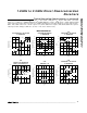
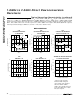
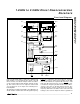
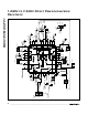
and output to 50Ω. The LNA in Figures 1 and 2 is
matched to 1960MHz and 2400MHz over a narrow
bandwidth.
I/Q Demodulator
The direct I/Q demodulator downconverts the RF signal
directly to baseband I and Q signals. This architec-
ture’s main advantage is that the received signal is
amplified and filtered at baseband rather than at some
high intermediate frequency. This eliminates the need
for an expensive IF SAW filter and the IF oscillator.
Furthermore, the direct conversion scheme eliminates
the need for image rejection, thereby relaxing the
bandpass filter selectivity requirements following the
LNA. The direct downconverter consists of highly linear
double-balanced I/Q mixers, an LO frequency doubler
option, an LO quadrature generator, and baseband I/Q
buffer amplifiers driven by the mixers’ outputs.
In a direct downconversion receiver, I/Q mixers have
more stringent requirements on mixer output linearity
since they need to handle large voltage swings at
baseband due to close-in interferers. The RF signal is
applied to the differential input (RFIN+, RFIN-) of the
direct downconversion receiver through an off-chip
balun. The differential input structure results in a higher
common-mode rejection for second-order nonlinearity
generated in the receiver’s front end. The differential
input requires matching to appropriate impedance of
the balun. Some applications may require a bandpass
filter between the LNA and the mixer, as shown in
Figures 1 and 2, to attenuate the residual transmit
power leakage and out-of-band spurious signals.
The mixer baseband buffers amplify the mixer I and Q
differential outputs and convert them to single-ended
outputs (MIX_I, MIX_Q). These buffer amplifiers have
PIN NAME FUNCTION
31 RFIN-
I/Q Mixers Noninverting Input. For narrow frequency bands between 1.8GHz and
2.5GHz, port must be matched using external matching components.
33 IOUT2 I-Channel VGA2 Baseband Output
34 DCI2- Inverting Offset Correction Input for I-Channel VGA2 Amplifier
35 DCI2+ Noninverting Offset Correction Input for I-Channel VGA2 Amplifier
36 IIN2- Inverting VGA2, I-Channel Baseband Input
37 IIN2+ Noninverting VGA2, I-Channel Baseband Input
39 IOUT1 I-Channel VGA1 Amplifier Baseband Output
40 DCI1- Inverting Offset Correction Input for I-Channel VGA1 Amplifier
41 DCI1+ Noninverting Offset Correction Input for I-Channel VGA1 Amplifier
42 IIN1- Inverting VGA1, I-Channel Baseband Input
43 IIN1+ Noninverting VGA1, I-Channel Baseband Input
45 MIX_I
Mixer I-Channel Baseband Output. Connect external series capacitor to AC-couple the
output to the load.
47 LO LO Input. Internally matched to 50Ω.
Pin Description (continued)