
User Manual


����������������������������������������������������������������� Maxim Integrated Products 6
MAX2670
GPS/GNSS Front-End Amplifier
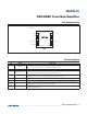
Pin Description
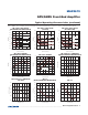
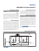
Pin Configuration
PIN NAME FUNCTION
1 RFIN2
Amplifier 2 Input. Incorporates an internal DC-blocking capacitor and is internally matched to
50I. This input is designed to be connected to a bandpass filter.
2, 3, 8, 9 GND Electrical Ground
4 EXTCAP/ALT_VCC
External Smoothing Capacitor for Internal Supply Voltage or Can Be Used as the External DC
Supply Pin to Eliminate the Need for a Bias-T on RFOUT2/VCC.
5 RFOUT2/VCC
Amplifier 2 Output. Incorporates an internal DC-blocking capacitor and is internally matched to
50I. DC bias on this pin serves as the power supply through a bias-T.
6 RFIN1 Amplifier 1 Input. Requires external DC-blocking capacitor and matching components.
7 GAIN_SELECT AMP 2 Gain Select. Open is high-gain mode. Short to ground is low-gain mode.
10 RFOUT1
Amplifier 1 Output. Incorporates an internal DC-blocking capacitor and is internally matched to
50I. This output is designed to drive a bandpass filter.
EP —
Exposed Pad Ground. The exposed pad must be soldered to the circuit board for proper thermal
and electrical performance.
1
+
3
4
10
8
7
RFOUT1
GND
GAIN_SELECT
RFIN2
GND
EXTCAP/ALT_VCC
2 9
GNDGND
5 6
RFIN1RFOUT2/VCC
EP
TDFN
TOP VIEW
MAX2670