
Manual


Detailed Description
The MAX2659 is an LNA designed for GPS L1,
GALILEO, and GLONASS applications. The device fea-
tures a power-shutdown control mode to eliminate the
need for an external supply switch. The device
achieves a 20.5dB gain and an ultra-low-noise figure of
0.8dB. The MAX2659 consumes approximately 4.1mA
while providing a IP
1dB
of -12dBm and an IIP3 of -5dBm.
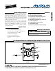
Input and Output Matching
The MAX2659 requires an off-chip input matching. Only
a 6.8nH inductor in series with a DC-blocking capacitor
is needed to form the input matching circuit. The
Typical Application Circuit
diagram shows the recom-
mended input-matching network. These values are
optimized for the best simultaneous gain, noise figure,
and return loss performance. Table 1 lists typical
device S11 values. The MAX2659 integrates an on-chip
output matching to 50Ω at the output, eliminating the
need for external matching components.
Shutdown
The MAX2659 includes a shutdown feature to turn off
the entire chip. Apply a logic high to SHDN pin to place
the part in the active mode and a logic low to place the
part in the shutdown mode.
Applications Information
A properly designed PC board (PCB) is essential to any
RF microwave circuit. Use controlled-impedance lines
on all high-frequency inputs and outputs. Bypass V
CC
with decoupling capacitors located close to the device.
For long V
CC
lines, it may be necessary to add decou-
pling capacitors. Locate these additional capacitors
further away from the device package. Proper ground-
ing of the GND pins is essential. If the PCB uses a top-
side RF ground, connect it directly to the GND pins. For
a board where the ground is not on the component
layer, connect the GND pins to the board with multiple
vias close to the package.
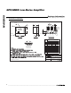
Chip Information
PROCESS: SiGe BiCMOS
MAX2659
GPS/GNSS Low-Noise Amplifier
_______________________________________________________________________________________ 5
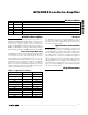
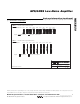
Pin Description
PIN NAME FUNCTION
1, 2 GND Ground. Connect to the PCB ground plane.
3 RFIN RF Input. Requires a DC-blocking capacitor and external matching components.
4 V
CC
Supply Voltage. Bypass to ground with a 33nF capacitor as close as possible to the IC.
5 SHDN Shutdown Input. A logic-low disables the device.
6 RFOUT RF Output. RFOUT is internally matched to 50 and incorporates an internal DC-blocking capacitor.
Table 1. Typical S11 Values
FREQUENCY (MHz) REAL S11 IMAGINARY S11
1000 -0.58 -j0.52
1100 -0.68 -j0.356
1200 -0.74 -j0.16
1300 -0.74 j0.036
1400 -0.676 j0.22
1500 -0.56 j0.36
1575 -0.47 j0.415
1600 -0.44 j0.43
1700 -0.36 j0.467
1800 -0.3 j0.51
1900 -0.228 j0.567
2000 -0.14 j0.622