
Owner's manual


MAX2657/MAX2658
GPS/GNSS Low-Noise Amplifiers
2 _______________________________________________________________________________________
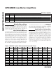
ABSOLUTE MAXIMUM RATINGS
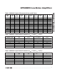
DC ELECTRICAL CHARACTERISTICS
(MAX2657/MAX2658 EV kit. V
CC
= 1.6V to 3.3V, T
A
= -40°C to +85°C, no RF signals are applied. Typical values are at V
CC
= 2.85V
and T
A
= +25°C, unless otherwise noted.) (Note 2)
Stresses beyond those listed under “Absolute Maximum Ratings” may cause permanent damage to the device. These are stress ratings only, and functional
operation of the device at these or any other conditions beyond those indicated in the operational sections of the specifications is not implied. Exposure to
absolute maximum rating conditions for extended periods may affect device reliability.
V
CC
to GND...........................................................-0.3V to +3.6V
Other Pins to GND .................-0.3V to (+ Operating V
CC
+ 0.3V)
Maximum RF Input Power ...............................................+5dBm
Continuous Power Dissipation (T
A
= +70°C)
6-Bump WLP (derates 10.5mW/°C above +70°C)........840mW
Maximum Current into RF Input ..........................................10mA
Operating Temperature Range ...........................-40°C to +85°C
Junction Temperature......................................................+150°C
Storage Temperature Range .............................-65°C to +160°C
Lead Temperature (soldering, 10s)..........Reflow Profile (Note 1)
PARAMETER CONDITIONS MIN TYP MAX UNITS
Supply Voltage 1.6 2.85 3.3 V
MAX2657 4.1
SHDN = high
MAX2658 7.7
mA
Supply Current
Shutdown mode, SHDN = low 1 µA
Digital Input Logic-High 1.2 V
Digital Input Logic-Low 0.45 V
Digital Input Current 1µA
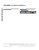
AC ELECTRICAL CHARACTERISTICS
(MAX2657/MAX2658 EV kit. V
CC
= 1.6V to 3.3V, T
A
= -40°C to +85°C, f
RFIN
= 1575.42MHz. Typical values are at V
CC
= 2.85V and
T
A
= +25°C, unless otherwise noted.) (Note 2)
PARAMETER CONDITIONS MIN TYP MAX UNITS
RF Frequency L1 band 1575.42 MHz
MAX2657 19.5
V
CC
= 2.85V
MAX2658 17.7
MAX2657 19.4
Power Gain
V
CC
= 1.6V
MAX2658 17.6
dB
V
CC
= 1.8V 0.8
Noise Figure
V
CC
= 3.3V 0.8
dB
MAX2657 -3.5
In-Band 3rd-Order Input Intercept
Point
(Note 3)
MAX2658 +4.5
dBm
MAX2657 +2.5
Out-of-Band 3rd-Order Input
Intercept Point
(Note 4)
MAX2658 +8
dBm
CAUTION! ESD SENSITIVE DEVICE
Note 1: Refer to Application Note 1891:
Wafer-Level Packaging (WLP) and Its Applications
.