
Instruction Manual

Detailed Description
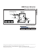
The MAX2203 RMS power detector is designed to
operate from 800MHz to 2.0GHz. The device is ideal for
WCDMA, cdma2000, and high-speed downlink/uplink
packet access. The MAX2203 accepts an RF signal at
the input and outputs the same voltage regardless of
the peak-average of the input signal. The output volt-
age and input power is linear in dB. The device has a
-24dBm to +3dBm detection range, and every dB
change in input power gives 35mV (typ) change in out-
put voltage. Table 1 shows the peak to average of the
signals used to test the MAX2203.
MAX2203
RMS Power Detector
_______________________________________________________________________________________ 5
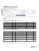
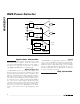
Pin Description
BUMP NAME FUNCTION
A1 RFIN/ENA
RF Input and Enable Logic Input. See the Typical Operating Circuit. Drive ENA high to turn on the
device. Drive ENA low to place it in shutdown mode.
A2, B1 GND Ground. Connect to PCB ground plane.
B2 FILT Intermediate Filtering Node. Bypass FILT with a capacitor as close as possible to the device.
C1 V
CC
Power Supply. Connect to either a regulated supply or battery. Bypass V
CC
with a capacitor as close
as possible to the device.
C2 OUT Detector Output. Connect an external lowpass RC filter for filtering.
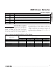
PAR AT DIFFERENT PROBABILITY OF COMPLEMENTARY CUMULATIVE
DISTRIBUTION (dB)
MODULATION
10% 1% 0.1% 0.01%
DPCCH + 1DPDCH 4.8 5.8 6.2 6.5
DPCCH + 5DPDCH 6.5 8.4 9.2 9.8
IS95 Reverse 5.5 6.9 7.6 8.1
IS95 Forward Pilot 5.6 7.6 8.8 9.5
9-Channel Forward 7 10.3 12 12.7
cdma2000 Pilot + DCCH 6.8 8.3 9.2 9.7
Table 1. Peak-to-Average Ratio (PAR*) of Test Signals
*
PAR of CW is 3dB.