
User Manual


MAX2102/MAX2105
Direct-Conversion Tuner ICs for
Digital DBS Applications
_______________________________________________________________________________________ 9
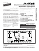
Pin Description
RF Ground. Connect directly to the ground plane.GND
9, 11,
19, 24
Automatic Gain-Control Input. Bypass this pin with a 1000pF capacitor close to the pin, to minimize cou-
pling.
AGC10
Q Channel Baseband OutputQOUT13
Baseband +5V Supply. Bypass with a 10pF capacitor from this pin to pin 12 (GND), as close to the IC as
possible. Connect an additional 0.1µF capacitor in parallel with the 10pF capacitor (placement less critical).
V
CC
14
Q Channel Offset-Correction Noninverting Input. Connect a 0.22µF (typ) capacitor between QDC and QDC.
This capacitor must be placed as close to the IC as possible (see
Layout Considerations
section).
QDC15
Ground (substrate)GND5
RF +5V Supply. Bypass with a 22pF capacitor from this pin to pin 9 (GND), as close to the IC as possible.V
CC
6
RF Noninverting Input. Couple through a 22pF capacitor directly to a 50Ω signal source.RFIN7
RF Inverting Input. Connect to a 22pF series capacitor and a 51Ω resistor to ground.
RFIN
8
RF +5V Supply. Bypass with a 22pF capacitor from this pin to pin 11 (GND), as close to the IC as possible.V
CC
4
Baseband GroundGND3, 12
PIN
I Channel Baseband OutputIOUT2
Baseband +5V Supply. Bypass with a 10pF capacitor from this pin to pin 3 (GND), as close to the IC as
possible. Connect an additional 0.1µF capacitor in parallel with the 10pF capacitor (placement less critical).
V
CC
1
FUNCTIONNAME
Q Channel Offset-Correction Inverting Input. Connect a 0.22µF (typ) capacitor between QDC and QDC. This
capacitor must be placed as close to the IC as possible (see
Layout Considerations
section).
QDC
16
I Channel Offset-Correction Inverting Input. Connect a 0.22µF (typ) capacitor between IDC and IDC. This
capacitor must be placed as close to the IC as possible (see
Layout Considerations
section).
IDC
17
I Channel Offset-Correction Noninverting Input. Connect a 0.22µF (typ) capacitor between IDC and IDC.
This capacitor must be placed as close to the IC as possible (see
Layout Considerations
section).
IDC18
RF +5V Supply. Bypass with a 10pF capacitor from this pin to pin 19 (GND) as close to the IC as possible.V
CC
20
Local-Oscillator Complementary Input Port (Figure 1)
LO
21
Local-Oscillator Input Port (Figure 1)LO22
RF +5V Supply. Bypass with a 10pF capacitor from this pin to pin 24 (GND) as close to the IC as possible.V
CC
23
Prescaler Ground. To disable the prescaler, leave this pin open.PSGND25
Prescaler Output. Drives CMOS load. Connect 2kΩ from this pin to GND (if the prescaler is enabled).PSOUT26
Prescaler Modulus Control. Leave open when the prescaler is disabled.MOD27
Prescaler +5V Supply. Must be connected even if the prescaler is disabled. Bypass with a 1000pF
capacitor.
V
CC
28